EVAL-AD9830EBZ Analog Devices Inc, EVAL-AD9830EBZ Datasheet - Page 9
EVAL-AD9830EBZ
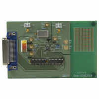
Manufacturer Part Number
EVAL-AD9830EBZ
Description
BOARD EVALUATION AD9830
Manufacturer
Analog Devices Inc
Specifications of EVAL-AD9830EBZ
Main Purpose
Timing, Direct Digital Synthesis (DDS)
Utilized Ic / Part
AD9830
Lead Free Status / RoHS Status
Lead free / RoHS Compliant
Secondary Attributes
-
Embedded
-
Primary Attributes
-
Lead Free Status / Rohs Status
Supplier Unconfirmed


REV. A
FREQ0 REG
FREQ1 REG
PHASE0 REG
PHASE1 REG
PHASE2 REG
PHASE3 REG
Register
Figure 18. AD9830 Control Registers
Size
32 Bits
32 Bits
12 Bits
12 Bits
12 Bits
12 Bits
Description
Frequency Register 0. This defines
the output frequency, when
FSELECT = 0, as a fraction of the
MCLK frequency.
Frequency Register 1. This de-
fines the output frequency, when
FSELECT = 1, as a fraction of the
MCLK frequency.
Phase Offset Register 0. When
PSEL0 = PSEL1 = 0, the contents
of this register are added to the out-
put of the phase accumulator.
Phase Offset Register 1. When
PSEL0 = 1 and PSEL1 = 0, the
contents of this register are added
to the output of the phase
accumulator.
Phase Offset Register 2. When
PSEL0 = 0 and PSEL1 = 1, the
contents of this register are added
to the output of the phase
accumulator.
Phase Offset Register 3. When
PSEL0 = PSEL1 = 1, the contents
of this register are added to the out-
put of the phase accumulator.
Figure 17. f
Word = 547AE148
START 0Hz
–10
–20
–30
–40
–50
–60
–70
–80
–90
0
RBW 1kHz
MCLK
= 50 MHz, f
VBW 3kHz
–9–
OUT
A2
0
0
0
0
1
1
1
1
D15 D14 D13 D12 D11
X
X = Don't Care
D15
MSB
= 16.5 MHz, Frequency
X
Figure 19. Addressing the Control Registers
X
A1
0
0
1
1
0
0
1
1
Figure 20. Frequency Register Bits
ST 50 SEC
STOP 25MHz
Figure 21. Phase Register Bits
X
MSB
A0
0
1
0
1
0
1
0
1
Destination Register
FREQ0 REG 16 LSBs
FREQ0 REG 16 MSBs
FREQ1 REG 16 LSBs
FREQ1 REG 16 MSBs
PHASE0 REG
PHASE1 REG
PHASE2 REG
PHASE3 REG
AD9830
D0
LSB
D0
LSB
Related parts for EVAL-AD9830EBZ
Image
Part Number
Description
Manufacturer
Datasheet
Request
R


Part Number:
Description:
BOARD EVAL FOR SI270X-A
Manufacturer:
Silicon Laboratories Inc
Datasheet:

Part Number:
Description:
BUCK CONV REF DESIGN KIT IP1201
Manufacturer:
International Rectifier
Datasheet:
Part Number:
Description:
BOARD DEMO SYNC DUAL BUCK CNVTER
Manufacturer:
International Rectifier
Datasheet:
Part Number:
Description:
BOARD DEMO SYNC BUCK CONVETER
Manufacturer:
International Rectifier
Datasheet:

Part Number:
Description:
EVALBOARD/EB Omnidirectional microphone - Analog
Manufacturer:
Analog Devices
Datasheet:
Part Number:
Description:
EVALBOARD/EB Omnidirectional microphone - Analog
Manufacturer:
Analog Devices
Datasheet:


Part Number:
Description:
BOARD EVAL LED DRIVER LT3756
Manufacturer:
Linear Technology
Datasheet:

Part Number:
Description:
BOARD EVAL FOR AD7741/7742
Manufacturer:
Analog Devices Inc
Datasheet:

Part Number:
Description:
±1.7g Dual-Axis IMEMS Accelerometer Evaluation Board
Manufacturer:
Analog Devices Inc
Datasheet:

Part Number:
Description:
IC MULTIPLIER ANALOG 8-SOIC T/R
Manufacturer:
Analog Devices Inc
Datasheet:

Part Number:
Description:
IC ANALOG MULTIPLIER 8-DIP
Manufacturer:
Analog Devices Inc
Datasheet:
Part Number:
Description:
IC ANALOG MULTIPLIER 8-SOIC
Manufacturer:
Analog Devices Inc
Datasheet:
Part Number:
Description:
IC ANALOG MULTIPLIER 8-DIP
Manufacturer:
Analog Devices Inc
Datasheet: