EVAL-ADUM4160EBZ Analog Devices Inc, EVAL-ADUM4160EBZ Datasheet - Page 3
EVAL-ADUM4160EBZ
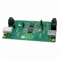
Manufacturer Part Number
EVAL-ADUM4160EBZ
Description
EVALUATION MODULE FOR ADUM4160
Manufacturer
Analog Devices Inc
Series
iCoupler®r
Datasheets
1.ADUM4160BRWZ-RL.pdf
(16 pages)
2.EVAL-ADUM4160EBZ.pdf
(8 pages)
3.EVAL-ADUM4160EBZ.pdf
(14 pages)
Specifications of EVAL-ADUM4160EBZ
Main Purpose
Interface, Digital Isolator
Embedded
No
Utilized Ic / Part
ADuM4160
Primary Attributes
USB Bidirectional Isolation
Secondary Attributes
3.1 V ~ 5.5 V Supply
Silicon Manufacturer
Analog Devices
Application Sub Type
USB Port Isolator
Kit Application Type
Interface
Silicon Core Number
ADuM4160
Lead Free Status / RoHS Status
Lead free / RoHS Compliant
Lead Free Status / RoHS Status
Lead free / RoHS Compliant, Lead free / RoHS Compliant
Other names
Q4508819


SPECIFICATIONS
ELECTRICAL CHARACTERISTICS
4.5 V ≤ V
the entire recommended operation range, unless otherwise noted; all typical specifications are at T
voltage is relative to its respective ground.
Table 1.
Parameter
DC SPECIFICATIONS
SWITCHING SPECIFICATIONS, I/O PINS LOW SPEED
SWITCHING SPECIFICATIONS, I/O PINS FULL SPEED
Total Supply Current
Idle Current
Input Currents
Single-Ended Logic High Input Threshold
Single-Ended Logic Low Input Threshold
Single-Ended Input Hysteresis
Differential Input Sensitivity
Logic High Output Voltages
Logic Low Output Voltages
V
V
V
Transceiver Capacitance
Capacitance Matching
Full Speed Driver Impedance
Impedance Matching
Low Speed Data Rate
Propagation Delay
Side 1 Output Rise/Fall Time (10% to 90%) Low
Low Speed Differential Jitter, Next Transition
Low Speed Differential Jitter, Paired Transition
Full Speed Data Rate
Propagation Delay
Output Rise/Fall Time (10% to 90%) Full Speed
Full Speed Differential Jitter, Next Transition
Full Speed Differential Jitter, Paired Transition
DD1
BUS1
BUS2
V
Speed
1.5 Mbps
12 Mbps
DD1
and V
V
V
V
V
Supply Undervoltage Lockout
Supply Undervoltage Lockout
DD1
DD2
DD1
DD2
or V
BUS1
or V
or V
or V
or V
DD2
BUS1
≤ 5.5 V, 4.5 V ≤ V
BUS1
BUS2
BUS1
BUS2
Supply Undervoltage Lockout
Idle Current
Supply Current
Supply Current
Supply Current
Supply Current
2
2
1
BUS2
≤ 5.5 V; 3.1 V ≤ V
DD1
Symbol
I
I
I
I
I
I
I
I
I
V
V
V
V
V
V
V
V
V
C
Z
t
t
|t
|t
t
t
|t
|t
DD1 (L)
DD2 (L)
DD1 (F)
DD2 (F)
DD1 (I)
DD−
UD+
SPD
SPU
PHLL
RL
PHLF
RF
IH
IL
HST
DI
OH
OL
UVLO
UVLOB1
UVLOB2
OUTH
LJN
LJP
FJN
FJP
IN
/t
/t
, I
, I
|
, I
, I
|
≤ 3.6 V, 3.1 V ≤ V
|
|
, t
FL
, t
FF
PIN
PDEN
DD+
UD−
PLHL
PLHF
,
,
,
Rev. B | Page 3 of 16
Min
−1
2.0
0.2
2.8
0
2.4
3.5
3.5
4
75
20
4
DD2
Typ
5
5
6
6
1.7
+0.1
0.4
10
10
10
1.5
45
15
12
60
3
1
≤ 3.6 V; all minimum/maximum specifications apply over
Max
7
7
8
8
2.3
+1
0.8
3.6
0.3
3.1
4.35
4.4
20
325
300
70
20
Unit
mA
mA
mA
mA
mA
µA
V
V
V
V
V
V
V
V
V
pF
%
Ω
%
Mbps C
ns
ns
ns
ns
Mbps C
ns
ns
ns
ns
A
= 25°C, V
Test Conditions
750 kHz logic signal rate C
750 kHz logic signal rate C
6 MHz logic signal rate C
6 MHz logic signal rate C
0 V ≤ V
V
|V
R
R
UD+, UD−, DD+, DD− to ground
C
V
C
V
C
C
C
V
C
V
C
C
SPU
L
L
L
L
DD2
L
DD2
L
L
L
L
DD2
L
DD2
L
L
XD+
= 15 kΩ, V
= 1.5 kΩ, V
= 50 pF
= 50 pF, SPD = SPU = low V
= 450 pF SPD = SPU = low V
= 50 pF
= 50 pF
= 50 pF
= 50 pF SPD = SPU = high, V
= 50 pF SPD = SPU = high, V
= 50 pF
= 50 pF
, V
= 3.3 V
= 3.3 V
= 3.3 V
= 3.3 V
− V
PDEN
DD-
DD1
XD−
, V
≤ 3.0
|
= V
DD+
L
L
= 0 V
= 3.6 V
, V
DD2
UD+
= 3.3 V. Each
ADuM4160
,V
UD−
, V
L
L
= 50 pF
= 50 pF
L
L
SPD
= 450 pF
= 450 pF
, V
DD1
DD1
DD1
DD1
PIN
,
,
,
,
,
Related parts for EVAL-ADUM4160EBZ
Image
Part Number
Description
Manufacturer
Datasheet
Request
R

Part Number:
Description:
EVAL BD For QSOP & SOIC16 Dig Isolators
Manufacturer:
Analog Devices Inc
Datasheet:

Part Number:
Description:
IC, ADJ LDO REG, 1.5V TO 5V 250mA MSOP-8
Manufacturer:
Vishay
Datasheet:

Part Number:
Description:
IC, ADJ LDO REG, 1.5V TO 5V 0.6A 8-TSSOP
Manufacturer:
Vishay
Datasheet:
Part Number:
Description:
IC, ADJ LDO REG, 1.5V TO 5V 250mA MSOP-8
Manufacturer:
Vishay
Datasheet:

Part Number:
Description:
IC ADJ LDO REG 1.5V TO 5V 150mA 5-SOT-23
Manufacturer:
Vishay
Datasheet:

Part Number:
Description:
BOARD EVAL AS1324-AD
Manufacturer:
austriamicrosystems
Datasheet:
Part Number:
Description:
IC, ADJ LDO REG, 1.5V TO 5V 0.6A 8-TSSOP
Manufacturer:
Vishay
Datasheet:

Part Number:
Description:
IC, ADJ LDO REG, 1.5V TO 5V, 0.3A, MSOP8
Manufacturer:
Vishay
Datasheet:
Part Number:
Description:
IC, ADJ LDO REG, 1.5V TO 5V, 0.3A, MSOP8
Manufacturer:
Vishay
Datasheet:
Part Number:
Description:
IC, ADJ LDO REG 1.215V TO 5V 0.3A MSOP-8
Manufacturer:
Vishay
Datasheet:

Part Number:
Description:
±1.7g Dual-Axis IMEMS Accelerometer Evaluation Board
Manufacturer:
Analog Devices Inc
Datasheet:

Part Number:
Description:
IC MULTIPLIER ANALOG 8-SOIC T/R
Manufacturer:
Analog Devices Inc
Datasheet:
Part Number:
Description:
IC ANALOG MULTIPLIER 8-DIP
Manufacturer:
Analog Devices Inc
Datasheet:
Part Number:
Description:
IC ANALOG MULTIPLIER 8-SOIC
Manufacturer:
Analog Devices Inc
Datasheet:
Part Number:
Description:
IC ANALOG MULTIPLIER 8-DIP
Manufacturer:
Analog Devices Inc
Datasheet: