EVAL-ADUM4160EBZ Analog Devices Inc, EVAL-ADUM4160EBZ Datasheet - Page 11
EVAL-ADUM4160EBZ
Manufacturer Part Number
EVAL-ADUM4160EBZ
Description
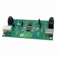
EVALUATION MODULE FOR ADUM4160
Manufacturer
Analog Devices Inc
Series
iCoupler®r
Datasheets
1.ADUM4160BRWZ-RL.pdf
(16 pages)
2.EVAL-ADUM4160EBZ.pdf
(8 pages)
3.EVAL-ADUM4160EBZ.pdf
(14 pages)
Specifications of EVAL-ADUM4160EBZ
Main Purpose
Interface, Digital Isolator
Embedded
No
Utilized Ic / Part
ADuM4160
Primary Attributes
USB Bidirectional Isolation
Secondary Attributes
3.1 V ~ 5.5 V Supply
Silicon Manufacturer
Analog Devices
Application Sub Type
USB Port Isolator
Kit Application Type
Interface
Silicon Core Number
ADuM4160
Lead Free Status / RoHS Status
Lead free / RoHS Compliant
Lead Free Status / RoHS Status
Lead free / RoHS Compliant, Lead free / RoHS Compliant
Other names
Q4508819


In a fully compliant application, a downstream facing port must
be able to detect whether a peripheral is low speed or full speed
based on the application of the upstream pull-up. The buffers
and logic conventions must adjust to match the requested speed.
Because the ADuM4160 sets its speed by hard wiring pins, the
part cannot adjust to different peripherals on the fly.
The practical result of using the ADuM4160 in a host port is
that the port works at a single speed. This behavior is acceptable
in embedded host applications; however, this type of interface is
not fully compliant as a general-purpose USB port.
Isolated cable applications have a similar issue. The cable operates
at the preset speed only; therefore, treat cable assemblies as
custom applications, not general-purpose isolated cables.
POWER SUPPLY OPTIONS
In most USB transceivers, 3.3 V is derived from the 5 V USB
bus through an LDO regulator. The ADuM4160 includes internal
LDO regulators on both the upstream and downstream sides.
The output of the LDO is available on the V
In some cases, especially on the peripheral side of the isolation,
there may not be a 5 V power supply available. The ADuM4160
has the ability to bypass the regulator and run on a 3.3 V supply
directly.
Two power pins are present on each side, V
is supplied to V
the xD+ and xD− drivers. V
3.3 V supply to allow external bypass as well as bias for external
pull-ups. If only 3.3 V is available, it can be supplied to both
V
coupler directly from the 3.3 V supply.
Figure 5 shows how to configure a typical application when the
upstream side of the coupler receives power directly from the
USB bus and the downstream side is receiving 3.3 V from the
peripheral power supply. The downstream side can run from a
5V V
manner as V
BUSx
BUS2
and V
power supply as well. It can be connected in the same
DDx
BUS1
. This disables the regulator and powers the
BUSx
as shown in Figure 5, if needed.
, an internal regulator creates 3.3 V to power
DDx
provides external access to the
BUSx
DD1
and V
and V
DD2
DDx
. If 5 V
pins.
Rev. B | Page 11 of 16
PRINTED CIRCUIT BOARD LAYOUT (PCB)
The ADuM4160 digital isolator requires no external interface
circuitry for the logic interfaces. For full speed operation, the
D+ and D− line on each side of the device requires a 24 Ω ± 1%
series termination resistor. These resistors are not required for
low speed applications. Power supply bypassing is required at
the input and output supply pins (Figure 5). Install bypass
capacitors between V
capacitor value should have a value of 0.1 µF and be of a low
ESR type. The total lead length between both ends of the
capacitor and the power supply pin should not exceed 10 mm.
Bypassing between Pin 2 and Pin 8 and between Pin 9 and
Pin 15 should also be considered, unless the ground pair on
each package side is connected close to the package.
In applications involving high common-mode transients, it is
important to minimize board coupling across the isolation
barrier. Furthermore, design the board layout such that any
coupling that does occur equally affects all pins on a given
component side. Failure to ensure this can cause voltage
differentials between pins exceeding the absolute maximum
ratings of the device, thereby leading to latch-up or permanent
damage.
DC CORRECTNESS AND MAGNETIC FIELD
IMMUNITY
Positive and negative logic transitions at the isolator input
cause narrow (~1 ns) pulses to be sent to the decoder via the
transformer. The decoder is bistable and is, therefore, either set
or reset by the pulses, indicating input logic transitions. In the
absence of logic transitions at the input for more than about
12 USB bit times, a periodic set of refresh pulses indicative of
the correct input state are sent to ensure dc correctness at the
output. If the decoder receives no internal pulses for more than
about 36 USB bit times, the input side is assumed to be unpowered
or nonfunctional, in which case the isolator output is forced to a
default state (see Table 10) by the watchdog timer circuit.
The limitation on the magnetic field immunity of the ADuM4160
is set by the condition in which induced voltage in the receiving
V
PDEN
GND
GND
V
BUS1
V
V
SPU
UD–
UD+
DD1
BUS1
DD1
Figure 5. Recommended Printed Circuit Board Layout
1
1
= 3.3V OUTPUT
= 5.0V INPUT
BUSx
and V
ADuM4160
DDx
on each side of the chip. The
V
V
BUS2
DD2
= 3.3V INPUT
= 3.3V INPUT
ADuM4160
V
GND
V
SPD
PIN
DD–
DD+
GND
BUS2
DD2
2
2
Related parts for EVAL-ADUM4160EBZ
Image
Part Number
Description
Manufacturer
Datasheet
Request
R

Part Number:
Description:
EVAL BD For QSOP & SOIC16 Dig Isolators
Manufacturer:
Analog Devices Inc
Datasheet:

Part Number:
Description:
IC, ADJ LDO REG, 1.5V TO 5V 250mA MSOP-8
Manufacturer:
Vishay
Datasheet:

Part Number:
Description:
IC, ADJ LDO REG, 1.5V TO 5V 0.6A 8-TSSOP
Manufacturer:
Vishay
Datasheet:
Part Number:
Description:
IC, ADJ LDO REG, 1.5V TO 5V 250mA MSOP-8
Manufacturer:
Vishay
Datasheet:

Part Number:
Description:
IC ADJ LDO REG 1.5V TO 5V 150mA 5-SOT-23
Manufacturer:
Vishay
Datasheet:

Part Number:
Description:
BOARD EVAL AS1324-AD
Manufacturer:
austriamicrosystems
Datasheet:
Part Number:
Description:
IC, ADJ LDO REG, 1.5V TO 5V 0.6A 8-TSSOP
Manufacturer:
Vishay
Datasheet:

Part Number:
Description:
IC, ADJ LDO REG, 1.5V TO 5V, 0.3A, MSOP8
Manufacturer:
Vishay
Datasheet:
Part Number:
Description:
IC, ADJ LDO REG, 1.5V TO 5V, 0.3A, MSOP8
Manufacturer:
Vishay
Datasheet:
Part Number:
Description:
IC, ADJ LDO REG 1.215V TO 5V 0.3A MSOP-8
Manufacturer:
Vishay
Datasheet:

Part Number:
Description:
±1.7g Dual-Axis IMEMS Accelerometer Evaluation Board
Manufacturer:
Analog Devices Inc
Datasheet:

Part Number:
Description:
IC MULTIPLIER ANALOG 8-SOIC T/R
Manufacturer:
Analog Devices Inc
Datasheet:
Part Number:
Description:
IC ANALOG MULTIPLIER 8-DIP
Manufacturer:
Analog Devices Inc
Datasheet:
Part Number:
Description:
IC ANALOG MULTIPLIER 8-SOIC
Manufacturer:
Analog Devices Inc
Datasheet:
Part Number:
Description:
IC ANALOG MULTIPLIER 8-DIP
Manufacturer:
Analog Devices Inc
Datasheet: