V2DIP1-32 FTDI, Future Technology Devices International Ltd, V2DIP1-32 Datasheet - Page 13
V2DIP1-32
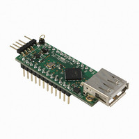
Manufacturer Part Number
V2DIP1-32
Description
MOD MCU-USB HOST CTLR 24-DIP
Manufacturer
FTDI, Future Technology Devices International Ltd
Series
Vinculum-IIr
Datasheet
1.V2DIP1-32.pdf
(21 pages)
Specifications of V2DIP1-32
Main Purpose
Interface, USB 2.0 Host/Controller
Embedded
Yes, ASIC
Utilized Ic / Part
VNC2-32Q
Primary Attributes
Single A-Type Connector, UART / Parallel FIFO / SPI Interfaces
Secondary Attributes
Second USB Port is Available via Pins, Traffic LEDs
Lead Free Status / RoHS Status
Lead free / RoHS Compliant
Other names
768-1058


3.7 Debugger Interface
The purpose of the debugger interface is to provide access to the VNC2 silicon/firmware debugger. The
debug interface can be accessed via the J2-10 pin on the DIL connector or, more easily, it can be
accessed by connecting a VNC2_Debug_Module to the J3 connector. This debug module will give access
to the debugger through a USB connection to a PC via the Integrated Development Environment (IDE).
The IDE is a graphical interface to the VNC2 software development tool-chain and gives the following
debug capabilities through the debugger interface:
The Debugger Interface, and how to use it, is further described in the following applications Note
Vinculum-II Debug Interface Description
3.7.1 Signal Description - Debugger Interface
Table 3.8
Table 3.8 - Signal Name and Description – Debugger Interface
J3-1
J3-2
J3-3
J3-4
J3-5
J3-6
Pin No.
Flash Erase, Write and Program.
Application debug - application code can have breakpoints, be single stepped and can be halted.
Detailed internal debug - memory and register read/write access.
shows the signals and pins description for the Debugger Interface pin header J3
RESET#
PROG#
Name
GND
IO0
5V0
-
Copyright © 2010 Future Technology Devices International Limited
On PCB
Name
`
PRG#
[Key]
RST#
DBG
GND
VCC
PWR Input
V2DIP1-32 VNC2-32Q Development Module Datasheet Version 1.01
Type
Input
Input
PWR
I/O
-
Can be used by an external device to reset the
VNCL2. This pin is also used in combination with
PROG# and the UART interface to program
firmware into the VNC2.
This pin is used in combination with the RESET#
pin and the UART interface to program firmware
into the VNC2.
5.0V module supply pin. This pin can be used to
provide the 5.0V input to the V2DIP1-32 from the
debugger interface when the V2DIP1-32 is not
powered from the USB connector (VBUS) or the
DIL connector pins J1-1 and J3-6.
Not connected. Used to make sure that the debug
module is connected correctly.
Module ground supply pin
Debugger Interface
Description
Document Reference No.: FT_000163
Clearance No.: FTDI# 150
12
Related parts for V2DIP1-32
Image
Part Number
Description
Manufacturer
Datasheet
Request
R

Part Number:
Description:
MOD MCU-USB HOST CTLR 24-DIP
Manufacturer:
FTDI, Future Technology Devices International Ltd
Datasheet:

Part Number:
Description:
MOD MCU-USB HOST CTLR 60-DIP
Manufacturer:
FTDI, Future Technology Devices International Ltd
Datasheet:

Part Number:
Description:
IC USB TO SERIAL UART 32-QFN
Manufacturer:
FTDI, Future Technology Devices International Ltd

Part Number:
Description:
IC USB HOST CTLR VINCULUM 48LQFP
Manufacturer:
FTDI, Future Technology Devices International Ltd
Datasheet:

Part Number:
Description:
IC USB HOST VINCULUM-II 32QFN
Manufacturer:
FTDI, Future Technology Devices International Ltd
Datasheet:
Part Number:
Description:
IC USB HOST VINCULUM-II 32LQFN
Manufacturer:
FTDI, Future Technology Devices International Ltd
Datasheet:
Part Number:
Description:
IC USB HOST VINCULUM-II 48QFN
Manufacturer:
FTDI, Future Technology Devices International Ltd
Datasheet:
Part Number:
Description:
IC USB HOST VINCULUM-II 32LQFN
Manufacturer:
FTDI, Future Technology Devices International Ltd
Datasheet:
Part Number:
Description:
IC USB HOST VINCULUM-II 32QFN
Manufacturer:
FTDI, Future Technology Devices International Ltd
Datasheet:
Part Number:
Description:
IC USB HOST VINCULUM-II 48LQFP
Manufacturer:
FTDI, Future Technology Devices International Ltd
Datasheet:
Part Number:
Description:
IC USB HOST VINCULUM-II 48LQFP
Manufacturer:
FTDI, Future Technology Devices International Ltd
Datasheet:
Part Number:
Description:
IC USB HOST VINCULUM-II 48QFN
Manufacturer:
FTDI, Future Technology Devices International Ltd
Datasheet:
Part Number:
Description:
IC USB HOST CTLR VINCULUM 64QFN
Manufacturer:
FTDI, Future Technology Devices International Ltd
Datasheet:

Part Number:
Description:
IC USB HOST CTLR VINCULUM 64LQFP
Manufacturer:
FTDI, Future Technology Devices International Ltd
Datasheet:
Part Number:
Description:
IC USB HOST VINCULUM-II 64LQFP
Manufacturer:
FTDI, Future Technology Devices International Ltd
Datasheet: