74LVC2G66EVB NXP Semiconductors, 74LVC2G66EVB Datasheet - Page 14
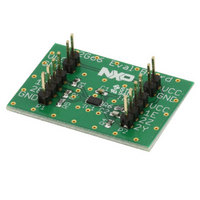
74LVC2G66EVB
Manufacturer Part Number
74LVC2G66EVB
Description
BOARD EVALUATION FOR 74LVC2G66
Manufacturer
NXP Semiconductors
Specifications of 74LVC2G66EVB
Main Purpose
Interface, Analog Switch
Embedded
No
Utilized Ic / Part
74LVC2G66
Primary Attributes
Dual SPST Analog Switch
Secondary Attributes
1.65 ~ 5.5 V Supply
Lead Free Status / RoHS Status
Lead free / RoHS Compliant
Other names
568-5081


NXP Semiconductors
Table 12.
At recommended operating conditions; voltages are referenced to GND (ground = 0 V); T
74LVC2G66
Product data sheet
Symbol Parameter
V
Xtalk
Q
ct
inj
crosstalk voltage
crosstalk
charge injection
Additional dynamic characteristics
Conditions
between digital inputs and switch; R
C
between switches; R
f
between switches; R
f
C
R
i
i
All information provided in this document is subject to legal disclaimers.
L
= 1 MHz; see
= 1 MHz; see
L
L
V
V
V
V
V
V
V
V
V
V
V
V
V
V
V
V
V
= 50 pF; f
= 0.1 nF; V
= 1 MΩ; see
CC
CC
CC
CC
CC
CC
CC
CC
CC
CC
CC
CC
CC
CC
CC
CC
CC
= 1.65 V
= 2.3 V
= 3.0 V
= 4.5 V
= 1.65 V
= 2.3 V
= 3 V
= 4.5 V
= 1.65 V
= 2.3 V
= 3 V
= 4.5 V
= 1.8 V
= 2.5 V
= 3.3 V
= 4.5 V
= 5.5 V
…continued
Rev. 5 — 16 June 2010
i
= 1 MHz; t
gen
Figure 24
Figure 24
Figure 25
= 0 V; R
L
L
= 600 Ω; C
= 50 Ω; C
r
= t
gen
f
= 2 ns; see
= 0 Ω; f
L
L
= 5 pF;
= 50 pF;
L
i
= 600 Ω;
= 1 MHz;
Figure 23
amb
= 25
Min Typ
-
-
-
-
-
-
-
-
-
-
-
-
-
-
-
-
-
74LVC2G66
°
C.
-
91
119
205
-
−56
−56
−56
-
−29
−28
−28
3.3
4.1
5.0
6.4
7.5
© NXP B.V. 2010. All rights reserved.
Bilateral switch
Max
-
-
-
-
-
-
-
-
-
-
-
-
-
-
-
-
-
14 of 26
Unit
mV
mV
mV
mV
dB
dB
dB
dB
dB
dB
dB
dB
pC
pC
pC
pC
pC
Related parts for 74LVC2G66EVB
Image
Part Number
Description
Manufacturer
Datasheet
Request
R

Part Number:
Description:
IC TRANSCVR TRI-ST DL 24SOIC
Manufacturer:
NXP Semiconductors
Datasheet:

Part Number:
Description:
IC ADDRESS/CLK DRIVER 56-TSSOP
Manufacturer:
IDT, Integrated Device Technology Inc
Datasheet:

Part Number:
Description:
IC MUX/DEMUX 2X1 6TSOP
Manufacturer:
NXP Semiconductors
Datasheet:

Part Number:
Description:
IC SWITCH QUAD SPST 14SOIC
Manufacturer:
NXP Semiconductors
Datasheet:

Part Number:
Description:
IC BUFF DVR TRI-ST 16BIT 48TSSOP
Manufacturer:
IDT, Integrated Device Technology Inc
Datasheet:

Part Number:
Description:
IC BUFF HEX OPEN DRAIN 14TSSOP
Manufacturer:
NXP Semiconductors
Datasheet:
Part Number:
Description:
IC BUFF HEX OPEN DRAIN 14SOICN
Manufacturer:
NXP Semiconductors
Datasheet:
Part Number:
Description:
IC BUFF DVR TRI-ST QD 14SSOP
Manufacturer:
NXP Semiconductors
Datasheet:
Part Number:
Description:
IC BUFF DVR TRI-ST QD 14SOICN
Manufacturer:
NXP Semiconductors
Datasheet:
Part Number:
Description:
IC BUFF DVR TRI-ST QD 14SOICN
Manufacturer:
NXP Semiconductors
Datasheet:
Part Number:
Description:
IC BUFF DVR TRI-ST QD 14SSOP
Manufacturer:
NXP Semiconductors
Datasheet:
Part Number:
Description:
IC BUFF DVR TRI-ST QD 14TSSOP
Manufacturer:
NXP Semiconductors
Datasheet:

Part Number:
Description:
IC BUFF/DVR TRI-ST DUAL 20SSOP
Manufacturer:
NXP Semiconductors
Datasheet:

Part Number:
Description:
IC BUFF/DVR TRI-ST DUAL 20SOIC
Manufacturer:
NXP Semiconductors
Datasheet:

Part Number:
Description:
IC BUFF/DVR TRI-ST DUAL 20TSSOP
Manufacturer:
NXP Semiconductors
Datasheet: