74LVC2G66EVB NXP Semiconductors, 74LVC2G66EVB Datasheet - Page 12
74LVC2G66EVB
Manufacturer Part Number
74LVC2G66EVB
Description
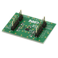
BOARD EVALUATION FOR 74LVC2G66
Manufacturer
NXP Semiconductors
Specifications of 74LVC2G66EVB
Main Purpose
Interface, Analog Switch
Embedded
No
Utilized Ic / Part
74LVC2G66
Primary Attributes
Dual SPST Analog Switch
Secondary Attributes
1.65 ~ 5.5 V Supply
Lead Free Status / RoHS Status
Lead free / RoHS Compliant
Other names
568-5081


NXP Semiconductors
Table 11.
74LVC2G66
Product data sheet
Supply voltage
V
1.65 V to 1.95 V
2.3 V to 2.7 V
2.7 V
3.0 V to 3.6 V
4.5 V to 5.5 V
Fig 19. Test circuit for measuring switching times
CC
Test data is given in
Definitions for test circuit:
R
C
R
V
EXT
L
L
T
Test data
= Load resistor.
= Load capacitance including jig and probe capacitance.
= Termination resistance should be equal to output impedance Z
= Test voltage for switching times.
Input
V
V
V
2.7 V
2.7 V
V
Table
I
CC
CC
CC
11.
negative
positive
pulse
pulse
GENERATOR
0 V
0 V
t
≤ 2.0 ns
≤ 2.0 ns
≤ 2.5 ns
≤ 2.5 ns
≤ 2.5 ns
V
V
r
, t
I
I
PULSE
All information provided in this document is subject to legal disclaimers.
f
90 %
10 %
t
t
Rev. 5 — 16 June 2010
f
r
Load
C
30 pF
30 pF
50 pF
50 pF
50 pF
V
V
L
M
M
V
10 %
90 %
I
R T
V
DUT
t
t
R
1 kΩ
500 Ω
500 Ω
500 Ω
500 Ω
W
W
CC
L
o
of the pulse generator.
V
O
V
V
M
M
V
t
open
open
open
open
open
PLH,
t
t
r
f
EXT
C L
001aae235
t
V
PHL
EXT
R L
R L
t
GND
GND
GND
GND
GND
PZH,
74LVC2G66
t
PHZ
© NXP B.V. 2010. All rights reserved.
Bilateral switch
t
2 × V
2 × V
6 V
6 V
2 × V
PZL,
t
CC
CC
CC
PLZ
12 of 26
Related parts for 74LVC2G66EVB
Image
Part Number
Description
Manufacturer
Datasheet
Request
R

Part Number:
Description:
IC TRANSCVR TRI-ST DL 24SOIC
Manufacturer:
NXP Semiconductors
Datasheet:

Part Number:
Description:
IC ADDRESS/CLK DRIVER 56-TSSOP
Manufacturer:
IDT, Integrated Device Technology Inc
Datasheet:

Part Number:
Description:
IC MUX/DEMUX 2X1 6TSOP
Manufacturer:
NXP Semiconductors
Datasheet:

Part Number:
Description:
IC SWITCH QUAD SPST 14SOIC
Manufacturer:
NXP Semiconductors
Datasheet:

Part Number:
Description:
IC BUFF DVR TRI-ST 16BIT 48TSSOP
Manufacturer:
IDT, Integrated Device Technology Inc
Datasheet:

Part Number:
Description:
IC BUFF HEX OPEN DRAIN 14TSSOP
Manufacturer:
NXP Semiconductors
Datasheet:
Part Number:
Description:
IC BUFF HEX OPEN DRAIN 14SOICN
Manufacturer:
NXP Semiconductors
Datasheet:
Part Number:
Description:
IC BUFF DVR TRI-ST QD 14SSOP
Manufacturer:
NXP Semiconductors
Datasheet:
Part Number:
Description:
IC BUFF DVR TRI-ST QD 14SOICN
Manufacturer:
NXP Semiconductors
Datasheet:
Part Number:
Description:
IC BUFF DVR TRI-ST QD 14SOICN
Manufacturer:
NXP Semiconductors
Datasheet:
Part Number:
Description:
IC BUFF DVR TRI-ST QD 14SSOP
Manufacturer:
NXP Semiconductors
Datasheet:
Part Number:
Description:
IC BUFF DVR TRI-ST QD 14TSSOP
Manufacturer:
NXP Semiconductors
Datasheet:

Part Number:
Description:
IC BUFF/DVR TRI-ST DUAL 20SSOP
Manufacturer:
NXP Semiconductors
Datasheet:

Part Number:
Description:
IC BUFF/DVR TRI-ST DUAL 20SOIC
Manufacturer:
NXP Semiconductors
Datasheet:

Part Number:
Description:
IC BUFF/DVR TRI-ST DUAL 20TSSOP
Manufacturer:
NXP Semiconductors
Datasheet: