74LVC2G66EVB NXP Semiconductors, 74LVC2G66EVB Datasheet - Page 11
74LVC2G66EVB
Manufacturer Part Number
74LVC2G66EVB
Description
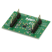
BOARD EVALUATION FOR 74LVC2G66
Manufacturer
NXP Semiconductors
Specifications of 74LVC2G66EVB
Main Purpose
Interface, Analog Switch
Embedded
No
Utilized Ic / Part
74LVC2G66
Primary Attributes
Dual SPST Analog Switch
Secondary Attributes
1.65 ~ 5.5 V Supply
Lead Free Status / RoHS Status
Lead free / RoHS Compliant
Other names
568-5081


NXP Semiconductors
Table 10.
74LVC2G66
Product data sheet
Supply voltage
V
1.65 V to 1.95 V
2.3 V to 2.7 V
2.7 V
3.0 V to 3.6 V
4.5 V to 5.5 V
Fig 17. Input (nY or nZ) to output (nZ or nY) propagation delays
Fig 18. Enable and disable times
CC
Σ{(C
L
+ C
Measurement points are given in
Logic levels: V
Measurement points are given in
Logic levels: V
Measurement points
S(ON)
11.1 Waveforms and test circuit
) × V
CC
OL
OL
2
nY or nZ
nY or nZ
× f
and V
and V
o
} = sum of the outputs.
Input
V
0.5 × V
0.5 × V
1.5 V
1.5 V
0.5 × V
OH
OH
M
HIGH-to-OFF
OFF-to-HIGH
LOW-to-OFF
OFF-to-LOW
are typical output voltage levels that occur with the output load.
are typical output voltage levels that occur with the output load.
nE input
output
output
nY or nZ
nZ or nY
CC
CC
CC
output
input
Table
Table
All information provided in this document is subject to legal disclaimers.
GND
GND
V
V
V
10.
10.
OH
GND
CC
OL
V
V
V
OH
I
OL
V
I
Rev. 5 — 16 June 2010
Output
V
0.5 × V
0.5 × V
1.5 V
1.5 V
0.5 × V
M
V
enabled
switch
M
t
V
t
PLZ
PHZ
M
V
CC
CC
CC
M
t
PLH
V
X
V
Y
disabled
switch
V
V
V
V
V
V
V
M
X
OL
OL
OL
OL
OL
001aaa541
V
M
+ 0.15 V
+ 0.15 V
+ 0.3 V
+ 0.3 V
+ 0.3 V
t
t
PHL
PZL
t
PZH
V
M
V
001aaa542
M
enabled
switch
74LVC2G66
V
V
V
V
V
V
Y
OH
OH
OH
OH
OH
© NXP B.V. 2010. All rights reserved.
Bilateral switch
− 0.15 V
− 0.15 V
− 0.3 V
− 0.3 V
− 0.3 V
11 of 26
Related parts for 74LVC2G66EVB
Image
Part Number
Description
Manufacturer
Datasheet
Request
R

Part Number:
Description:
IC TRANSCVR TRI-ST DL 24SOIC
Manufacturer:
NXP Semiconductors
Datasheet:

Part Number:
Description:
IC ADDRESS/CLK DRIVER 56-TSSOP
Manufacturer:
IDT, Integrated Device Technology Inc
Datasheet:

Part Number:
Description:
IC MUX/DEMUX 2X1 6TSOP
Manufacturer:
NXP Semiconductors
Datasheet:

Part Number:
Description:
IC SWITCH QUAD SPST 14SOIC
Manufacturer:
NXP Semiconductors
Datasheet:

Part Number:
Description:
IC BUFF DVR TRI-ST 16BIT 48TSSOP
Manufacturer:
IDT, Integrated Device Technology Inc
Datasheet:

Part Number:
Description:
IC BUFF HEX OPEN DRAIN 14TSSOP
Manufacturer:
NXP Semiconductors
Datasheet:
Part Number:
Description:
IC BUFF HEX OPEN DRAIN 14SOICN
Manufacturer:
NXP Semiconductors
Datasheet:
Part Number:
Description:
IC BUFF DVR TRI-ST QD 14SSOP
Manufacturer:
NXP Semiconductors
Datasheet:
Part Number:
Description:
IC BUFF DVR TRI-ST QD 14SOICN
Manufacturer:
NXP Semiconductors
Datasheet:
Part Number:
Description:
IC BUFF DVR TRI-ST QD 14SOICN
Manufacturer:
NXP Semiconductors
Datasheet:
Part Number:
Description:
IC BUFF DVR TRI-ST QD 14SSOP
Manufacturer:
NXP Semiconductors
Datasheet:
Part Number:
Description:
IC BUFF DVR TRI-ST QD 14TSSOP
Manufacturer:
NXP Semiconductors
Datasheet:

Part Number:
Description:
IC BUFF/DVR TRI-ST DUAL 20SSOP
Manufacturer:
NXP Semiconductors
Datasheet:

Part Number:
Description:
IC BUFF/DVR TRI-ST DUAL 20SOIC
Manufacturer:
NXP Semiconductors
Datasheet:

Part Number:
Description:
IC BUFF/DVR TRI-ST DUAL 20TSSOP
Manufacturer:
NXP Semiconductors
Datasheet: