MCP3909RD-1PH1 Microchip Technology, MCP3909RD-1PH1 Datasheet - Page 29
MCP3909RD-1PH1
Manufacturer Part Number
MCP3909RD-1PH1
Description
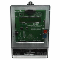
BOARD DES MCP3909 ENERGY METER
Manufacturer
Microchip Technology
Datasheets
1.MCP3909T-ISS.pdf
(44 pages)
2.MCP3909RD-1PH1.pdf
(60 pages)
3.MCP3909RD-1PH1.pdf
(6 pages)
Specifications of MCP3909RD-1PH1
Main Purpose
Power Management, Energy/Power Meter
Embedded
Yes, MCU, 8-Bit
Utilized Ic / Part
MCP3909, PIC18F85J90
Primary Attributes
Single Phase Shunt Energy Meter
Secondary Attributes
16 Bit ADC
Ic Function
Single Phase Energy Measurement IC
Supply Voltage Range
4.5V To 5.5V
Operating Temperature Range
-40°C To +85°C
Digital Ic Case Style
SSOP
No. Of Pins
24
Interface Type
SPI
Lead Free Status / RoHS Status
Contains lead / RoHS non-compliant
Lead Free Status / RoHS Status
Contains lead / RoHS non-compliant


3.5.13
3.5.14
3.5.15
© 2009 Microchip Technology Inc.
bit 15
bit 7
Legend:
R = Readable bit
-n = Value at POR
bit 15-2
bit 1
bit 0
W_GAIN
DELAY
R/W-0
R/W-0
MODE1_DEF
PHA_CAL_Status Register
STANDARD_W_RAW
CALIBRATION REGISTER: Calibration register status for offset, gain, LSB, and phase delay
1 = This register has been calibrated
0 = This register is NOT calibrated
Unimplemented: Read as ‘0’
STANDARD: Standard Phase Bit
1 = Standard Phase is THIS phase
0 = This phase is NOT the standard phase
I_RMS_OFF
W_GLSB
R/W-0
R/W-0
REGISTER 3-24:
Mode 1 default power-up settings. On power-up, this register will be read and placed
into the MOD1 register.
REGISTER 3-25:
The PHASE_A CAL_STATUS registers holds the calibration status for each individual
phase. Broken down by phase, these are the values that can be calibrated. Each bit
has the status of ‘0’ = Not calibrated, ‘1’ = Calibrated.
REGISTER 3-26:
This calibration register holds the energy value that was accumulated during the
standard phase measurement under calibration configuration C1. The software will
read this value when performing phase to phase gain matching during active power
calibration.
STANDARD_W_RAW
MODE1_DEF
PHA_CAL_STATUS
W = Writable bit
‘1’ = Bit is set
V_RMS_OFF
Name
VA_GAIN
R/W-0
R/W-0
Name
Name
Calculation and Register Description
I_RMS_GAIN V_RMS_GAIN
PHA_CAL_STATUS REGISTER
MODE1_DEF REGISTER
VA_GLSB
STANDARD_W_RAW REGISTER
R/W-0
R/W-0
Bits
16
Bits
48
Bits
16
Address
U = Unimplemented bit, read as ‘0’
‘0’ = Bit is cleared
0x1B0
VAR_GAIN
Address
0x1B8
R/W-0
R/W-0
Address
0x1B2
R/W
Cof
I_RMS_GLSB
R/W
Cof
VAR_GLSB
R/W-0
R/W-0
R/W
Cof
x = Bit is unknown
V_RMS_GLSB
R/W-0
U-0
—
DS51884A-page 29
STANDARD
W_OFF
R/W-0
R/W-0
bit 8
bit 0
Related parts for MCP3909RD-1PH1
Image
Part Number
Description
Manufacturer
Datasheet
Request
R

Part Number:
Description:
REF DESIGN FOR MCP3909 W/18F2520
Manufacturer:
Microchip Technology
Datasheet:

Part Number:
Description:
REF DESIGN MCP3909 3PH ENGY MTR
Manufacturer:
Microchip Technology
Datasheet:

Part Number:
Description:
Manufacturer:
Microchip Technology Inc.
Datasheet:
Part Number:
Description:
Manufacturer:
Microchip Technology Inc.
Datasheet:
Part Number:
Description:
Manufacturer:
Microchip Technology Inc.
Datasheet:
Part Number:
Description:
Manufacturer:
Microchip Technology Inc.
Datasheet:
Part Number:
Description:
Manufacturer:
Microchip Technology Inc.
Datasheet:
Part Number:
Description:
Manufacturer:
Microchip Technology Inc.
Datasheet:
Part Number:
Description:
Manufacturer:
Microchip Technology Inc.
Datasheet:
Part Number:
Description:
Manufacturer:
Microchip Technology Inc.
Datasheet: