MCP3421DM-BFG Microchip Technology, MCP3421DM-BFG Datasheet - Page 4
MCP3421DM-BFG
Manufacturer Part Number
MCP3421DM-BFG
Description
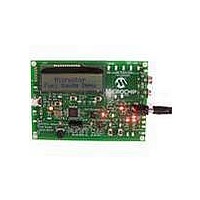
BOARD DEMO FOR MCP3421
Manufacturer
Microchip Technology
Datasheets
1.MCP3421A2T-ECH.pdf
(42 pages)
2.MCP3421DM-BFG.pdf
(26 pages)
3.MCP3421A0T-ECH.pdf
(30 pages)
Specifications of MCP3421DM-BFG
Main Purpose
Power Management, Battery Gauge
Utilized Ic / Part
MCP3421
Processor To Be Evaluated
MCP3421
Lead Free Status / RoHS Status
Lead free / RoHS Compliant
Secondary Attributes
-
Embedded
-
Primary Attributes
-
Lead Free Status / RoHS Status
Lead free / RoHS Compliant, Lead free / RoHS Compliant


MCP3421
ELECTRICAL CHARACTERISTICS (CONTINUED)
DS22003E-page 4
Electrical Specifications: Unless otherwise specified, all parameters apply for T
V
Gain Error (Note 5)
PGA Gain Error Match (Note 5)
Gain Error Drift (Note 5)
Offset Error
Offset Drift vs. Temperature
Common-Mode Rejection
Gain vs. V
Power Supply Rejection at DC
Power Requirements
Voltage Range
Supply Current during
Conversion
Supply Current during Standby
Mode
I
High level input voltage
Low level input voltage
Low level output voltage
Hysteresis of Schmitt Trigger
for inputs (Note 7)
Supply Current when I
line is active
Input Leakage Current
Pin Capacitance and I
Pin capacitance
I
Note 1:
2
2
IN
C Digital Inputs and Digital Outputs
C Bus Capacitance
+ = V
2:
3:
4:
5:
6:
7:
8:
IN
Parameters
DD
- = V
Any input voltage below or greater than this voltage causes leakage current through the ESD diodes at the input pins.
This parameter is ensured by characterization and not 100% tested.
This input impedance is due to 3.2 pF internal input sampling capacitor.
The total conversion speed includes auto-calibration of offset and gain.
INL is the difference between the endpoints line and the measured code at the center of the quantization band.
Includes all errors from on-board PGA and V
Full Scale Range (FSR) = 2 x 2.048/PGA = 4.096/PGA.
This parameter is ensured by characterization and not 100% tested.
This parameter is ensured by design and not 100% tested.
REF
/2. All ppm units use 2*V
2
2
C bus
C Bus Capacitance
V
Sym
C
I
I
I
V
V
V
V
HYST
I
DDA
DDS
V
DDB
I
C
ILH
ILL
PIN
OS
DD
OL
IH
IL
b
REF
0.05V
0.7 V
as full scale range.
Min
2.7
—
—
—
—
—
—
—
—
—
—
—
—
—
—
—
—
—
—
-1
DD
DD
REF
.
0.05
105
110
100
155
145
Typ
0.1
0.1
50
15
15
—
—
—
—
—
—
—
—
—
—
5
0.3V
0.35
V
Max
190
400
5.5
0.5
0.4
40
10
10
—
—
—
—
—
—
—
—
—
—
DD
1
DD
A
= -40°C to +85°C, V
ppm/°C
ppm/V
nV/°C
Units
µV
dB
dB
dB
µA
µA
µA
µA
µA
µA
pF
pF
%
%
V
V
V
V
V
© 2009 Microchip Technology Inc.
PGA = 1, DR = 3.75 SPS
Between any 2 PGA gains
PGA=1, DR=3.75 SPS
Tested at PGA = 1
V
V
at DC and PGA =1,
at DC and PGA =8,
T
T
PGA = 1
T
PGA = 1
V
V
I
f
V
V
OL
SCL
A
A
A
DD
DD
DD
DD
IH
IL
= +25°C
= +25°C, V
= +25°C, V
= 3 mA, V
= GND
= 5.5V
DD
= 5.0V
= 5.0V and DR = 3.75 SPS
= 5.0V
= 3.0V
= 100 kHz
= +5.0V, V
DD
DD
DD
Conditions
= +5.0V
= 2.7V to 5.5V,
= 2.7V to 5.5V,
SS
= 0V,
Related parts for MCP3421DM-BFG
Image
Part Number
Description
Manufacturer
Datasheet
Request
R

Part Number:
Description:
18-Bit Analog-to-Digital Converter with I2C Interface and On-Board Reference
Manufacturer:
Microchip Technology
Datasheet:

Part Number:
Description:
Manufacturer:
Microchip Technology Inc.
Datasheet:
Part Number:
Description:
Manufacturer:
Microchip Technology Inc.
Datasheet:
Part Number:
Description:
Manufacturer:
Microchip Technology Inc.
Datasheet:
Part Number:
Description:
Manufacturer:
Microchip Technology Inc.
Datasheet:
Part Number:
Description:
Manufacturer:
Microchip Technology Inc.
Datasheet:
Part Number:
Description:
Manufacturer:
Microchip Technology Inc.
Datasheet:
Part Number:
Description:
Manufacturer:
Microchip Technology Inc.
Datasheet:
Part Number:
Description:
Manufacturer:
Microchip Technology Inc.
Datasheet: