MCP3421DM-BFG Microchip Technology, MCP3421DM-BFG Datasheet - Page 13
MCP3421DM-BFG
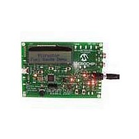
Manufacturer Part Number
MCP3421DM-BFG
Description
BOARD DEMO FOR MCP3421
Manufacturer
Microchip Technology
Datasheets
1.MCP3421A2T-ECH.pdf
(42 pages)
2.MCP3421DM-BFG.pdf
(26 pages)
3.MCP3421A0T-ECH.pdf
(30 pages)
Specifications of MCP3421DM-BFG
Main Purpose
Power Management, Battery Gauge
Utilized Ic / Part
MCP3421
Processor To Be Evaluated
MCP3421
Lead Free Status / RoHS Status
Lead free / RoHS Compliant
Secondary Attributes
-
Embedded
-
Primary Attributes
-
Lead Free Status / RoHS Status
Lead free / RoHS Compliant, Lead free / RoHS Compliant


4.9
4.9.1
The digital output code is proportional to the input
voltage and PGA settings. The output data format is a
binary two’s complement. With this code scheme, the
MSB can be considered a sign indicator. When the
MSB is a logic ‘0’, the input is positive. When the MSB
is a logic ‘1’, the input is negative. The following is an
example of the output code:
a.
b.
c.
The MSB (sign bit) is always transmitted first through
the I
conversion is 18, 16, 14, or 12 bits depending on the
conversion rate selection bit settings by the user.
The output codes will not roll-over even if the input volt-
age exceeds the maximum input range. In this case,
the code will be locked at 0111...11 for all voltages
greater than (V
voltages less than -V
example of output codes of various input levels for 18
bit conversion mode.
minimum and maximum output codes for each
conversion rate option.
The number of output code is given by:
EQUATION 4-2:
The LSB of the data conversion is given by:
EQUATION 4-3:
© 2009 Microchip Technology Inc.
Number of Output Code
Where:
Where:
for a negative full scale input voltage:
100...000
Example: (V
for a zero differential input voltage: 000...000
Example: (V
for
011...111
Example: (V
2
=
N = User programmable bit resolution:
See
C serial data line. The resolution for each
(
Digital Output Codes and
Conversion to Real Values
Maximum Code
a
Table 4-3
DIGITAL OUTPUT CODE FROM
DEVICE
LSB
12,14,16, or 18
positive
REF
IN
IN
IN
=
+ - V
+ - V
+ - V
- 1 LSB)/PGA and 1000...00 for
2 V
--------------------- -
for Maximum Code.
×
Table 4-3
REF
2
IN
IN
IN
full
N
+
REF
-)
-) = 0
-)
1
/PGA.
•
•
) PGA
PGA = -2.048V
PGA = 2.048V
×
scale
=
2 2.048V
--------------------------
shows an example of
Table 4-2
×
×
2
input
N
(
---------------------------------- -
V
IN
2.048V
+ V
voltage:
shows an
–
IN
-
)
Table 4-1
setting. The measured unknown input voltage is
obtained by multiplying the output codes with LSB. See
the following section for the input voltage calculation
using the output codes.
TABLE 4-1:
TABLE 4-2:
TABLE 4-3:
Note 1:
Resolution
Note:
[V
Setting
Input Voltage:
IN
Resolution Setting
V
12
14
16
18
+ - V
2:
REF
< -V
-1 LSB
-2 LSB
≥
- V
2 LSB
1 LSB
shows the LSB size of each conversion rate
V
- 1 LSB
MSB is a sign indicator:
0: Positive input (V
1: Negative input (V
Output data format is binary two’s
complement.
IN
0
Maximum n-bit code = 2
Minimum n-bit code = -1 x 2
REF
REF
12 bits
14 bits
16 bits
18 bits
REF
-] • PGA
Data Rate
3.75 SPS
240 SPS
60 SPS
15 SPS
RESOLUTION SETTINGS VS.
LSB
EXAMPLE OF OUTPUT CODE
FOR 18 BITS (NOTE 1,NOTE 2)
MINIMUM AND MAXIMUM
OUTPUT CODES (NOTE)
011111111111111111
011111111111111111
000000000000000010
000000000000000001
000000000000000000
111111111111111111
111111111111111110
100000000000000000
100000000000000000
Minimum
Digital Output Code
-131072
-32768
MCP3421
-2048
-8192
IN
Code
IN
+ > V
+ < V
N-1
DS22003E-page 13
15.625 µV
IN
IN
62.5 µV
250 µV
-)
- 1
N-1
1 mV
-)
LSB
Maximum
131071
32767
Code
8191
2047
Related parts for MCP3421DM-BFG
Image
Part Number
Description
Manufacturer
Datasheet
Request
R

Part Number:
Description:
18-Bit Analog-to-Digital Converter with I2C Interface and On-Board Reference
Manufacturer:
Microchip Technology
Datasheet:

Part Number:
Description:
Manufacturer:
Microchip Technology Inc.
Datasheet:
Part Number:
Description:
Manufacturer:
Microchip Technology Inc.
Datasheet:
Part Number:
Description:
Manufacturer:
Microchip Technology Inc.
Datasheet:
Part Number:
Description:
Manufacturer:
Microchip Technology Inc.
Datasheet:
Part Number:
Description:
Manufacturer:
Microchip Technology Inc.
Datasheet:
Part Number:
Description:
Manufacturer:
Microchip Technology Inc.
Datasheet:
Part Number:
Description:
Manufacturer:
Microchip Technology Inc.
Datasheet:
Part Number:
Description:
Manufacturer:
Microchip Technology Inc.
Datasheet: