MCP3421DM-BFG Microchip Technology, MCP3421DM-BFG Datasheet - Page 19
MCP3421DM-BFG
Manufacturer Part Number
MCP3421DM-BFG
Description
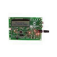
BOARD DEMO FOR MCP3421
Manufacturer
Microchip Technology
Datasheets
1.MCP3421A2T-ECH.pdf
(42 pages)
2.MCP3421DM-BFG.pdf
(26 pages)
3.MCP3421A0T-ECH.pdf
(30 pages)
Specifications of MCP3421DM-BFG
Main Purpose
Power Management, Battery Gauge
Utilized Ic / Part
MCP3421
Processor To Be Evaluated
MCP3421
Lead Free Status / RoHS Status
Lead free / RoHS Compliant
Secondary Attributes
-
Embedded
-
Primary Attributes
-
Lead Free Status / RoHS Status
Lead free / RoHS Compliant, Lead free / RoHS Compliant


5.3.3
When the Master sends a read command (R/W = 1),
the device outputs both the conversion data and config-
uration bytes. Each byte consists of 8 bits with one
acknowledge (ACK) bit. The ACK bit after the address
byte is issued by the device and the ACK bits after each
conversion data bytes are issued by the Master.
When the device is configured for 18-bit conversion
mode, it outputs three data bytes followed by a
configuration byte. The first 6 data bits in the first data
byte are repeated MSB (= sign bit) of the conversion
data. The user can ignore the first 6 data bits, and take
the 7th data bit (D17) as the MSB of the conversion
data. The LSB of the 3rd data byte is the LSB of the
conversion data (D0).
If the device is configured for 12, 14, or 16 bit-mode, the
device outputs two data bytes followed by a
configuration byte. In 16 bit-conversion mode, the MSB
(= sign bit) of the first data byte is D15. In 14-bit
conversion mode, the first two bits in the first data byte
are repeated MSB bits and can be ignored, and the 3rd
bit (D13) is the MSB (=sign bit) of the conversion data.
In 12-bit conversion mode, the first four bits are
repeated MSB bits and can be ignored. The 5th bit
(D11) of the byte represents the MSB (= sign bit) of the
conversion data.
data output of each conversion mode.
TABLE 5-3:
© 2009 Microchip Technology Inc.
Note 1:
Conversion
Option
18-bits
16-bits
14-bits
12-bits
2:
3:
4:
D17 is MSB (= sign bit), M is repeated MSB of the data byte.
D15 is MSB (= sign bit).
D13 is MSB (= sign bit), M is repeated MSB of the data byte.
D11 is MSB (= sign bit), M is repeated MSB of the data byte.
READING OUTPUT CODES AND
CONFIGURATION BYTE FROM THE
DEVICE
MMMMMMD17D16 (1st data byte) - D15 ~ D8 (2nd data byte) - D7 ~ D0 (3rd data byte) - Configuration
byte. (Note 1)
D15 ~ D8 (1st data byte) - D7 ~ D0 (2nd data byte) - Configuration byte. (Note 2)
MMD13D ~ D8 (1st data byte) - D7 ~ D0 (2nd data byte) - Configuration byte. (Note 3)
MMMMD11 ~ D8 (1st data byte) - D7 ~ D0 (2nd data byte) - Configuration byte. (Note 4)
Table 5-3
OUTPUT CODES OF EACH RESOLUTION OPTION
summarizes the conversion
Digital Output Codes
The configuration byte follows the output data bytes.
The device repeatedly outputs the configuration byte
only if the Master sends clocks repeatedly after the
data bytes.
The device terminates the current outputs when it
receives a Not-Acknowledge (NAK), a repeated start or
a stop bit at any time during the output bit stream. It is
not required to read the configuration byte. However,
the Master may read the configuration byte to check
the RDY bit condition.The Master may continuously
send clock (SCL) to repeatedly read the configuration
byte (to check the RDY bit status).
Figures 5-3
reading.
and
5-4
show the timing diagrams of the
MCP3421
DS22003E-page 19
Related parts for MCP3421DM-BFG
Image
Part Number
Description
Manufacturer
Datasheet
Request
R

Part Number:
Description:
18-Bit Analog-to-Digital Converter with I2C Interface and On-Board Reference
Manufacturer:
Microchip Technology
Datasheet:

Part Number:
Description:
Manufacturer:
Microchip Technology Inc.
Datasheet:
Part Number:
Description:
Manufacturer:
Microchip Technology Inc.
Datasheet:
Part Number:
Description:
Manufacturer:
Microchip Technology Inc.
Datasheet:
Part Number:
Description:
Manufacturer:
Microchip Technology Inc.
Datasheet:
Part Number:
Description:
Manufacturer:
Microchip Technology Inc.
Datasheet:
Part Number:
Description:
Manufacturer:
Microchip Technology Inc.
Datasheet:
Part Number:
Description:
Manufacturer:
Microchip Technology Inc.
Datasheet:
Part Number:
Description:
Manufacturer:
Microchip Technology Inc.
Datasheet: