MCP3905RD-PM1 Microchip Technology, MCP3905RD-PM1 Datasheet - Page 15
MCP3905RD-PM1
Manufacturer Part Number
MCP3905RD-PM1
Description
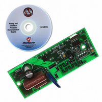
REFERENCE DESIGN FOR MCP3905
Manufacturer
Microchip Technology
Specifications of MCP3905RD-PM1
Main Purpose
Power Management, Energy/Power Meter
Embedded
No
Utilized Ic / Part
MCP3905/6
Primary Attributes
1-Phase, 220 VAC, In Case, With Mechanical Counter
Secondary Attributes
On Board Transformerless AC/DC 5V Supply
Silicon Manufacturer
Microchip
Silicon Core Number
MCP3905A,MCP3906A
Kit Application Type
Power Management
Application Sub Type
Energy Meter
Kit Contents
Design Guides
Lead Free Status / RoHS Status
Lead free / RoHS Compliant
Available stocks
Company
Part Number
Manufacturer
Quantity
Price
Company:

Part Number:
MCP3905RD-PM1
Manufacturer:
MICROCHIP
Quantity:
12 000


2.6
© 2009 Microchip Technology Inc.
BACK SIDE OF PCB DETAILED DESCRIPTION
2.5.5
These two connections feed the DC power supply circuitry described in
Section 2.6.3 “Metal Oxide Varistor (MOV1)”. JP4 is connected to the ground of the
PCB, and JP3 to the high-side of the DC power supply circuitry. JP3 is also connected
to the resistor divider that feeds the analog input of Channel 1 of the MCP3905A/06A.
This is the channel for measuring voltage and is connected to the differential input in a
single-ended fashion. See Appendix A. “Schematics and Layouts” for further detail.
2.6.1
From the back side of the board, the MCP3905A/06A is located on the right hand side
where the analog ground plane exists. The MCP3905A/06A has appropriate bypass
capacitors on V
its input logic pins connected to user-selectable jumpers, with the exception of the HPF
pin. For this system, the HPF is turned on with this pin connected to V
in AC mode only. The NEG connection is not connected in this reference design; this
pin should be left floating. The other three output pins (F
connected to nodes JP5, JP6 and JP7 described later in this section.
2.6.2
The DC power supply is created from a half-wave zener diode limited AC signal feeding
a 7805 +5V regulator. C17 and C16 divide the AC signal coming directly from the line
and designed in this document for 220V. The zener diode D2 limits the peak voltage to
15V.
2.6.3
A MOV is included to suppress any high voltage transients coming through the power
lines.
2.6.4
An optical isolator is included in the reference design as an additional level of protection
for other circuitry used in advanced meter designs (PICmicro
otherwise). It is connected to the HF
Depending on the meter design, it may not be required. This design is a direct-connect
meter that has the entire PCB referenced to the phase or line-side of the power supply.
Therefore, any other circuitry would either need to be biased to the same point or
isolated using this scheme. A pull-up resistor is required on the output of the optical
isolator to allow the HF logic signal to appear.
2.6.5
The MCP3905A/06A Energy Meter Reference Design PCB is designed for low-noise
performance and immunity to external influences, as required by IEC61036. The DC
power supply and digital outputs are connected to the power supply ground plane
(right-side of the board when looking at it from the front). The lower noise analog
ground plane, including the MCP3905A/06A connections, is on the opposite side of the
board, separated by a moat between the two ground planes. An inductive choke
connects the two grounds.
Connection to Voltage or Phase Line and Ground Reference
Point (JP3,JP4)
MCP3905A (U1)
DC Power Supply (C17, C16, U2, C18, D2)
Metal Oxide Varistor (MOV1)
Optical Isolator (U3)
The Analog Ground Plane, Power Supply Ground Plane, Moat.
DD
coming from the DC power supply circuitry. The MCP3905A/06A has
Installation and Operation
OUT
frequency output of the MCP3905A.
OUT0
®
, F
microcontroller, DSP or
OUT1
, HF
DD
DS51565B-page 11
; the device is
OUT
) are
Related parts for MCP3905RD-PM1
Image
Part Number
Description
Manufacturer
Datasheet
Request
R

Part Number:
Description:
IC ENERGY METER 24-SSOP
Manufacturer:
Microchip Technology
Datasheet:

Part Number:
Description:
Energy-Metering ICs with Active (Real) Power Pulse Output
Manufacturer:
Microchip Technology
Part Number:
Description:
(MCP3905 / MCP3906) Energy-Metering ICs
Manufacturer:
Microchip Technology
Datasheet:

Part Number:
Description:
Manufacturer:
Microchip Technology Inc.
Datasheet:
Part Number:
Description:
Manufacturer:
Microchip Technology Inc.
Datasheet:
Part Number:
Description:
Manufacturer:
Microchip Technology Inc.
Datasheet:
Part Number:
Description:
Manufacturer:
Microchip Technology Inc.
Datasheet:
Part Number:
Description:
Manufacturer:
Microchip Technology Inc.
Datasheet:
Part Number:
Description:
Manufacturer:
Microchip Technology Inc.
Datasheet:
Part Number:
Description:
Manufacturer:
Microchip Technology Inc.
Datasheet: