CP2400DK Silicon Laboratories Inc, CP2400DK Datasheet - Page 28
CP2400DK
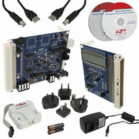
Manufacturer Part Number
CP2400DK
Description
KIT EVAL SPI LCD DRIVER CP2400
Manufacturer
Silicon Laboratories Inc
Specifications of CP2400DK
Main Purpose
LCD Development
Embedded
Yes
Utilized Ic / Part
CP2400
Primary Attributes
I²C, SMBus Interfaces
Secondary Attributes
Up to 128 segments
Product
Microcontroller Modules
Core Processor
C8051F930
Clock Speed
20 MHz
Interface Type
SPI
Timers
2
Operating Supply Voltage
1.8 V to 3.6 V
Cpu Core
C8051F930
Lead Free Status / RoHS Status
Contains lead / RoHS non-compliant
Lead Free Status / RoHS Status
Lead free / RoHS Compliant, Contains lead / RoHS non-compliant
Other names
336-1858
336-1858
336-1858


CP2400/1/2/3
28
Notes:
General:
Solder Mask Design:
Stencil Design:
Card Assembly:
1. All dimensions shown are in millimeters (mm) unless otherwise noted.
2. This Land Pattern Design is based on the IPC-7351 guidelines.
3. All metal pads are to be non-solder mask defined (NSMD). Clearance between
4. A stainless steel, laser-cut and electro-polished stencil with trapezoidal walls
5. The stencil thickness should be 0.125 mm (5 mils).
6. The ratio of stencil aperture to land pad size should be 1:1 for all pads.
7. A No-Clean, Type-3 solder paste is recommended.
8. The recommended card reflow profile is per the JEDEC/IPC J-STD-020
Figure 4.10. TQFP-48 Recommended PCB Land Pattern
the solder mask and the metal pad is to be 60 µm minimum, all the way around
the pad.
should be used to assure good solder paste release.
specification for Small Body Components.
Table 4.3. TQFP-48 PCB Land Pattern Dimensions
Dimension
C1
C2
X1
Y1
E
Rev. 1.0
8.30
8.30
0.20
1.40
Min
0.50 BSC
Max
8.40
8.40
0.30
1.50
Related parts for CP2400DK
Image
Part Number
Description
Manufacturer
Datasheet
Request
R

Part Number:
Description:
IC LCD DRIVER 48TQFP
Manufacturer:
Silicon Laboratories Inc
Datasheet:
Part Number:
Description:
IC LCD DRIVER 48QFN
Manufacturer:
Silicon Laboratories Inc
Datasheet:

Part Number:
Description:
SMD/C°/SINGLE-ENDED OUTPUT SILICON OSCILLATOR
Manufacturer:
Silicon Laboratories Inc
Part Number:
Description:
Manufacturer:
Silicon Laboratories Inc
Datasheet:
Part Number:
Description:
N/A N/A/SI4010 AES KEYFOB DEMO WITH LCD RX
Manufacturer:
Silicon Laboratories Inc
Datasheet:
Part Number:
Description:
N/A N/A/SI4010 SIMPLIFIED KEY FOB DEMO WITH LED RX
Manufacturer:
Silicon Laboratories Inc
Datasheet:
Part Number:
Description:
N/A/-40 TO 85 OC/EZLINK MODULE; F930/4432 HIGH BAND (REV E/B1)
Manufacturer:
Silicon Laboratories Inc
Part Number:
Description:
EZLink Module; F930/4432 Low Band (rev e/B1)
Manufacturer:
Silicon Laboratories Inc
Part Number:
Description:
I°/4460 10 DBM RADIO TEST CARD 434 MHZ
Manufacturer:
Silicon Laboratories Inc
Part Number:
Description:
I°/4461 14 DBM RADIO TEST CARD 868 MHZ
Manufacturer:
Silicon Laboratories Inc
Part Number:
Description:
I°/4463 20 DBM RFSWITCH RADIO TEST CARD 460 MHZ
Manufacturer:
Silicon Laboratories Inc
Part Number:
Description:
I°/4463 20 DBM RADIO TEST CARD 868 MHZ
Manufacturer:
Silicon Laboratories Inc
Part Number:
Description:
I°/4463 27 DBM RADIO TEST CARD 868 MHZ
Manufacturer:
Silicon Laboratories Inc
Part Number:
Description:
I°/4463 SKYWORKS 30 DBM RADIO TEST CARD 915 MHZ
Manufacturer:
Silicon Laboratories Inc