SI5356-EVB Silicon Laboratories Inc, SI5356-EVB Datasheet - Page 3
SI5356-EVB
Manufacturer Part Number
SI5356-EVB
Description
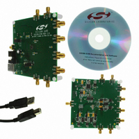
EVALUATION BOARD FOR SI5356
Manufacturer
Silicon Laboratories Inc
Specifications of SI5356-EVB
Main Purpose
Timing, Clock Generator
Utilized Ic / Part
SI5356
Technology Type
Evaluation Board
For Use With/related Products
Si5356
Lead Free Status / RoHS Status
Lead free / RoHS Compliant
Secondary Attributes
-
Embedded
-
Primary Attributes
-
Lead Free Status / Rohs Status
Lead free / RoHS Compliant
Other names
336-1750


2.1. Status LEDS
There are three status LEDs on the EVB:
2.2. Inputs
The Si5356 EVB provides two reference options - using the on-board XTAL or an external reference.
Note: Si5356-EVB Rev 1.0 does not support synchronous operation using the CLKIN input. This feature will be supported in
2.2.1. External Input reference
An SMA connector (CLKIN) is provided to receive an external single-ended CMOS signal. This input is dc-coupled
to the device. The signal should have a minimum amount of dc bias to ensure that it never swings below ground
level.
2.2.2. On-board XTAL
The on-board 25 MHz allows the Si5356 EVB to generate asynchronous clocks. To use this option, select the XTAL
input from the Si5356 “ClockBuilder Desktop” software.
2.3. Outputs (CLK0-CLK7)
Each of the eight output clocks can be accessed using SMA connectors. The outputs are dc-coupled (no in-line dc
blocking capacitors between the output pin and the SMA connector).
2.4. Control Pins
Header J7 located on the backside of the Si5356 EVB allows setting three Si5356 control pins: SSC_DIS,
I2C_LSB, and OEB.
2.4.1. SSC_DIS
This pin allows disabling of the spread spectrum feature on the output clocks. Spread spectrum is disabled when
the jumper is installed.
2.4.2. I2C_LSB
This pin is the least significant bit of the Si5356 I
I
jumper is not installed.
2.4.3. OEB
This pin allows disabling all output clocks. All outputs are enabled when the jumper is installed.
2.5. Voltage Regulators
The Si5356 EVB has five built-in programmable voltage regulators to allow setting of the VDD supply (to 3.3 V,
2.5 V, and 1.8 V) and the four VDDO supplies (to 3.3 V, 2.5 V, and 1.8 V). The voltage level on each of these
supplies can be set independently.
2.6. Reset Switch
A reset switch is provided to reset communication between the PC and Si5356 EVB.
2
C bus. I
RDY (Green) indicates that the EVB is operating as normal. This LED should always be on.
BUSY (Green) lights when there is active communication between the PC, the MCU, and the Si5356.
INTR (Red) indicates the MCU has detected that the interrupt pin of the Si5356 device is enabled. The most
probable cause for an interrupt is because the Si5356 has lost its input signal or the PLL has lost lock. The
“Status” tab of the GUI will identify the event that caused the interrupt to happen.
future revisions.
2
C address of the Si5356 = 0x70 when the jumper is installed. I
2
C address allowing up to two Si5356 devices to occupy the same
Rev. 0.2
2
C address of the Si5356 = 0x71 when the
Si5356-EVB
3
Related parts for SI5356-EVB
Image
Part Number
Description
Manufacturer
Datasheet
Request
R

Part Number:
Description:
SMD/C°/SINGLE-ENDED OUTPUT SILICON OSCILLATOR
Manufacturer:
Silicon Laboratories Inc
Part Number:
Description:
Manufacturer:
Silicon Laboratories Inc
Datasheet:
Part Number:
Description:
N/A N/A/SI4010 AES KEYFOB DEMO WITH LCD RX
Manufacturer:
Silicon Laboratories Inc
Datasheet:
Part Number:
Description:
N/A N/A/SI4010 SIMPLIFIED KEY FOB DEMO WITH LED RX
Manufacturer:
Silicon Laboratories Inc
Datasheet:
Part Number:
Description:
N/A/-40 TO 85 OC/EZLINK MODULE; F930/4432 HIGH BAND (REV E/B1)
Manufacturer:
Silicon Laboratories Inc
Part Number:
Description:
EZLink Module; F930/4432 Low Band (rev e/B1)
Manufacturer:
Silicon Laboratories Inc
Part Number:
Description:
I°/4460 10 DBM RADIO TEST CARD 434 MHZ
Manufacturer:
Silicon Laboratories Inc
Part Number:
Description:
I°/4461 14 DBM RADIO TEST CARD 868 MHZ
Manufacturer:
Silicon Laboratories Inc
Part Number:
Description:
I°/4463 20 DBM RFSWITCH RADIO TEST CARD 460 MHZ
Manufacturer:
Silicon Laboratories Inc
Part Number:
Description:
I°/4463 20 DBM RADIO TEST CARD 868 MHZ
Manufacturer:
Silicon Laboratories Inc
Part Number:
Description:
I°/4463 27 DBM RADIO TEST CARD 868 MHZ
Manufacturer:
Silicon Laboratories Inc
Part Number:
Description:
I°/4463 SKYWORKS 30 DBM RADIO TEST CARD 915 MHZ
Manufacturer:
Silicon Laboratories Inc
Part Number:
Description:
N/A N/A/-40 TO 85 OC/4463 RFMD 30 DBM RADIO TEST CARD 915 MHZ
Manufacturer:
Silicon Laboratories Inc
Part Number:
Description:
I°/4463 20 DBM RADIO TEST CARD 169 MHZ
Manufacturer:
Silicon Laboratories Inc