STEVAL-IPE009V1 STMicroelectronics, STEVAL-IPE009V1 Datasheet - Page 31
STEVAL-IPE009V1
Manufacturer Part Number
STEVAL-IPE009V1
Description
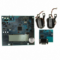
BOARD EVAL ST72321BR9/STPM14
Manufacturer
STMicroelectronics
Type
Other Power Managementr
Specifications of STEVAL-IPE009V1
Main Purpose
Power Management, Energy/Power Meter
Embedded
Yes, MCU, 8-Bit
Utilized Ic / Part
STPM14, ST72F321BR9T6
Primary Attributes
1-Ph 220 VAC, LCD Displays: No-Load, Reverse, Fraud, or Case Tampering
Secondary Attributes
Up to 4 Tariff Rates, Data Accumulated for Meter Life, Time Stamp for: Tamper, Fraud, Power Failure
Input Voltage
220 V
Product
Power Management Modules
Silicon Manufacturer
ST Micro
Silicon Core Number
ST72321BR9 And STPM14
Features
Continuously Detects, Displays No-Load Condition, Reverse Direction, Fraud And Case Tamper Condition
Lead Free Status / RoHS Status
Lead free / RoHS Compliant
For Use With/related Products
STPM14, ST72321BR9
Other names
497-8434
STEVAL-IPE009V1
STEVAL-IPE009V1


STPM11, STPM12, STPM13, STPM14
The condition in which SCS, SYN-NP and SCL-NLC inputs are set to high level determines
the idle state of the CFGI interface and no data transfer occurs.
Any pin above has internal weak pull up device of nominal 15 A. This means that when a pin
is not forced by external signals, the state of the pin is logic high. A high state of any input
pin above is considered as an idle (not active) state. For the CFGI to operate correctly, the
STPM1x must be correctly supplied as described in the power supply section. When SCS is
active (low), signal SDA-TD should change its state at trailing edge of signal SCL-NLC and
the signal SDA-TD should be stable at the next leading edge of signal SCL-NLC. The first
valid bit of SDA-TD always starts with the activation of signal SCL-NLC.
Writing procedure
Each writable bit (configuration and mode bits) has its own 6-bit absolute address. For the
configuration bits, the 6-bit address value corresponds to its decimal value, while for the
mode bits, the addresses are the ones indicated in the Mode Signal paragraph (7.16).
In order to change the latch state, a byte of data must be sent to STPM1x via CFGI. This
byte consists of 1-bit data to be latched (msb), followed by 6-bit address of destination latch,
followed by 1-bit don't care data (lsb) which totals 8 bits of command byte.
For example, if we would like to set the configuration bit 52 (additional gain of 8) to 1, we
must convert the decimal 52 to its 6-bit binary value: 110100. The byte command will be
then composed like this:
1 bit DATA value+6-bits address+1 bit (0 or 1) as depicted in
binary command will be 11101000 (0xE8) or 11101001 (0xE9).
– SCS: in the STPM1X, the SYN-NP, SCL-NLC and SDA-TD have the dual task to
– SYN-NP: this pin allows synchronization of the communication between STPM1x and
– SCL-NLC: it is basically the clock pin of the CFGI interface. This pin function is also
– SDA-TD is the Data pin. SDA-TD is the input of the serial bit data signal.
provide information on the meter status (see Pin Description table) and to allow CFGI
communication. The SCS pin allows using the above pins for CFGI communication
when it is low and allows the normal operation of SYN-NP, SCL-NLC and SDA-TD
when it is high. In this section, the SYN-NP, SCL-NLC and SDA-TD operation as part
of the CFGI interface is described.
the host. See
controlled by the SCS status. If SCS is low, SCL-NLC is the input of the serial bit
synchronization clock signal. When SCS is high, SCL-NLC is also high which
determines the idle state of the CFGI.
Figure 21
Doc ID 13167 Rev 7
- for detailed timing of the pin.
Figure
21. In this case the
Theory of operation
31/46
Related parts for STEVAL-IPE009V1
Image
Part Number
Description
Manufacturer
Datasheet
Request
R

Part Number:
Description:
BOARD DEMO TFT DISPLAY STR91
Manufacturer:
STMicroelectronics
Datasheet:

Part Number:
Description:
BOARD EVAL FOR MEMS SENSORS
Manufacturer:
STMicroelectronics
Datasheet:

Part Number:
Description:
KIT DEV STARTER ST10F276Z5
Manufacturer:
STMicroelectronics
Datasheet:

Part Number:
Description:
BOARD EVAL HDMI $ VIDEO SWITCH
Manufacturer:
STMicroelectronics
Datasheet:

Part Number:
Description:
BOARD DEMO ACCELEROMETER DIL24
Manufacturer:
STMicroelectronics
Datasheet:

Part Number:
Description:
BOARD STLM75/STDS75/ST72F651
Manufacturer:
STMicroelectronics
Datasheet:

Part Number:
Description:
EVAL BOARD 3AXIS MEMS ACCELLRMTR
Manufacturer:
STMicroelectronics
Datasheet:

Part Number:
Description:
BOARD EVAL 8BIT MICRO + TDE1708
Manufacturer:
STMicroelectronics
Datasheet:

Part Number:
Description:
EVAL BOARD A/D TS4657
Manufacturer:
STMicroelectronics
Datasheet:

Part Number:
Description:
BOARD ADAPTER 20DIP LIS3LV02DL
Manufacturer:
STMicroelectronics
Datasheet:
Part Number:
Description:
STMicroelectronics [RIPPLE-CARRY BINARY COUNTER/DIVIDERS]
Manufacturer:
STMicroelectronics
Datasheet:
Part Number:
Description:
STMicroelectronics [LIQUID-CRYSTAL DISPLAY DRIVERS]
Manufacturer:
STMicroelectronics
Datasheet:
Part Number:
Description:
BOARD EVAL FOR MEMS SENSORS
Manufacturer:
STMicroelectronics
Datasheet: