CY8CKIT-006 Cypress Semiconductor Corp, CY8CKIT-006 Datasheet - Page 4
CY8CKIT-006
Manufacturer Part Number
CY8CKIT-006
Description
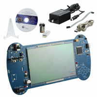
KIT DEV PSOC3 LCD SEGMENT
Manufacturer
Cypress Semiconductor Corp
Series
PSOC™ 3r
Specifications of CY8CKIT-006
Main Purpose
Displays, LCD Display
Embedded
Yes, MCU, 32-Bit
Primary Attributes
448 addressable segments
Secondary Attributes
Configurable LCD pin selection
Description/function
Evaluation Kit
Interface Type
USB
Backlighting
No Backlighting
Data Bus Width
8 bit, 16 bit, 32 bit
Maximum Operating Temperature
+ 50 C
Minimum Operating Temperature
0 C
Number Of Segments
7
Operating Supply Voltage
12 V
Operating Voltage
3.3 V
Pixel Format
16 x 28
Product
Display Modules
Software
Software Included
Touch Panel
No Touch Panel
For Use With/related Products
PSoC 3
Lead Free Status / RoHS Status
Lead free / RoHS Compliant
Utilized Ic / Part
-
Lead Free Status / Rohs Status
Lead free / RoHS Compliant
Other names
428-2994
Available stocks
Company
Part Number
Manufacturer
Quantity
Price
Company:

Part Number:
CY8CKIT-006
Manufacturer:
Cypress Semiconductor Corp
Quantity:
135


4
5.3
5.4
5.2.2
5.2.3
5.2.4
5.2.5
Project Design and Setup........................................................................................................................28
5.3.1
5.3.2
5.3.3
5.3.4
5.3.5
5.3.6
5.3.7
5.3.8
5.3.9
5.3.10 Real Time Clock (RTC) ..............................................................................................................57
5.3.11 EEPROM....................................................................................................................................60
5.3.12 System Clocks............................................................................................................................61
5.3.13 Pin Mapping ...............................................................................................................................62
5.3.14 Low Power Operation.................................................................................................................64
5.3.15 Low Power Entry ........................................................................................................................64
5.3.16 Automatic Low Power Entry .......................................................................................................65
5.3.17 Manual Low Power Entry ...........................................................................................................65
5.3.18 Periodic Wake and Return to Sleep ...........................................................................................65
5.3.19 Wake from Sleep ........................................................................................................................65
5.3.20 Low Power Exit...........................................................................................................................65
Source Code Description ........................................................................................................................66
5.4.1
Temperature Measurements ......................................................................................................26
5.2.2.1
RTC Crystal and Clocking ..........................................................................................................27
Contrast Adjustments .................................................................................................................28
LCD Demonstration....................................................................................................................28
Analog I/O ..................................................................................................................................28
5.3.1.1
5.3.1.2
5.3.1.3
5.3.1.4
5.3.1.5
Analog MUX ...............................................................................................................................34
VDAC .........................................................................................................................................34
Delta-Sigma ADC .......................................................................................................................35
PWM...........................................................................................................................................36
5.3.5.1
5.3.5.2
5.3.5.3
Timer ..........................................................................................................................................38
Timer 1 kHz Clock Source..........................................................................................................39
5.3.7.1
5.3.7.2
Segment LCD.............................................................................................................................41
5.3.8.1
5.3.8.2
5.3.8.3
Digital I/O....................................................................................................................................48
5.3.9.1
5.3.9.2
5.3.9.3
5.3.9.4
5.3.9.5
5.3.9.6
5.3.9.7
5.3.9.8
5.3.10.1
Top Level Functional Description ...............................................................................................66
5.4.1.1
5.4.1.2
5.4.1.3
5.4.1.4
5.4.1.5
5.4.1.6
CY8CKIT-006 PSoC 3 LCD Segment Drive Evaluation Kit Guide, Doc. # 001-52798 Rev. *C
Temperature Sensing Design Principle.....................................................................27
Thermistor Reference Voltage ..................................................................................28
Thermistor Signal Voltage.........................................................................................29
Accelerometer Y-Axis................................................................................................30
Accelerometer X-Axis................................................................................................31
Battery Monitor - 9V Level.........................................................................................32
PWM 6 kHz Clock Source.........................................................................................37
Logic High for PWM Kill Pin ......................................................................................38
Logic Low for PWM Reset Pin ..................................................................................38
Logic Level Low for Timer .........................................................................................40
Timer ISR ..................................................................................................................40
LCD Glass Character Pixel Mapping ........................................................................42
LCD Glass Icon Pixel Mapping .................................................................................46
Pixel Only Mapped Icons ..........................................................................................48
Sleep Button .............................................................................................................48
Sleep Button ISR ......................................................................................................50
Wall Supply (Vin) Detect ...........................................................................................51
VBus Detect ..............................................................................................................53
Digital Outputs...........................................................................................................54
Accelerometer On .....................................................................................................54
Buzzer In ...................................................................................................................55
Logic Level High for Buzzer In Output Enable ..........................................................56
CapSense Buttons ....................................................................................................57
Main Loop .................................................................................................................66
Punch Gauge Mode ..................................................................................................67
RTC/TEMP................................................................................................................68
Contrast Control Mode ..............................................................................................70
LCD Demonstration Mode.........................................................................................71
Register Descriptions ................................................................................................72
[+] Feedback
Related parts for CY8CKIT-006
Image
Part Number
Description
Manufacturer
Datasheet
Request
R

Part Number:
Description:
KIT DEV FOR PSOC3/5
Manufacturer:
Cypress Semiconductor Corp
Datasheet:

Part Number:
Description:
PSoC1/3/5 Development Kit
Manufacturer:
Cypress Semiconductor Corp
Datasheet:

Part Number:
Description:
KIT DEV PSOC PROC MODULE CY8C38
Manufacturer:
Cypress Semiconductor Corp

Part Number:
Description:
KIT DEV PSOC PROC MODULE CY8C29
Manufacturer:
Cypress Semiconductor Corp

Part Number:
Description:
KIT DEV PSOC ANALOG VOLTMETER
Manufacturer:
Cypress Semiconductor Corp
Datasheet:

Part Number:
Description:
KIT DEV PSOC5 FIRST TOUCH
Manufacturer:
Cypress Semiconductor Corp
Datasheet:

Part Number:
Description:
KIT DEV PSOC3 FIRSTTOUCH STARTER
Manufacturer:
Cypress Semiconductor Corp
Datasheet:
Part Number:
Description:
KIT DEV PROC MODULE PSOC5
Manufacturer:
Cypress Semiconductor Corp
Datasheet:

Part Number:
Description:
KIT PSOC CY8C28 FAMILY PROCESSOR
Manufacturer:
Cypress Semiconductor Corp
Datasheet:

Part Number:
Description:
KIT PSOC MINIPROG3 PROGRAM DEBUG
Manufacturer:
Cypress Semiconductor Corp
Datasheet:

Part Number:
Description:
KIT EVAL POWERLINE HIGH VOLT
Manufacturer:
Cypress Semiconductor Corp
Datasheet:

Part Number:
Description:
KIT PSOC FIRST TOUCH
Manufacturer:
Cypress Semiconductor Corp
Datasheet:

Part Number:
Description:
EVAL KIT WORLDTOUR2
Manufacturer:
Cypress Semiconductor Corp
Datasheet:

Part Number:
Description:
KIT UNIVERSAL CAPSENSE CTRLR
Manufacturer:
Cypress Semiconductor Corp
Datasheet:
