EVL6563S-400W STMicroelectronics, EVL6563S-400W Datasheet
EVL6563S-400W
Specifications of EVL6563S-400W
Available stocks


Related parts for EVL6563S-400W


EVL6563S-400W Summary of contents
Page 1
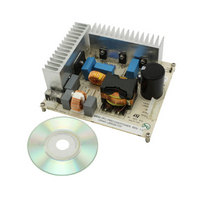
... L6563S, which is usually prohibitive at this power level. Fixed-off-time control allows continuous conduction mode operation, which is normally achieved with more expensive control chips and more complex control architectures. Figure 1. L6563S 400 W FOT PFC demonstration board (p/n EVL6563S-400W) November 2010 Application note Doc ID 15796 Rev 2 ...
Page 2
Contents Contents 1 Main characteristics and circuit description . . . . . . . . . . . . . . . . . . . . . 5 2 Test results and significant waveforms . . . . ...
Page 3
... EVL6563S-400W input mains dip from 140 to 90 Vac, full load, CFF = 1 µ Figure 26. L6562A FOT input mains dip from 140 to 90 Vac, full load, NO VFF input . . . . . . . . . . . . 17 Figure 27. EVL6563S-400W start- Vac, 60 Hz, full load . . . . . . . . . . . . . . . . . . . . . . . . . . . . . 18 Figure 28. EVL6563S-400W start-up at 265 Vac, 50 Hz, full load . . . . . . . . . . . . . . . . . . . . . . . . . . . . 18 Figure 29. ...
Page 4
... List of tables List of tables Table 1. Measured temperature at 115 Vac and 230 Vac - full load . . . . . . . . . . . . . . . . . . . . . . . . 29 Table 2. Bill of materials for the EVL6563S-400W demonstration board . . . . . . . . . . . . . . . . . . . . . 31 Table 3. Winding characteristics . . . . . . . . . . . . . . . . . . . . . . . . . . . . . . . . . . . . . . . . . . . . . . . . . . . . 34 Table 4. Document revision history . . . . . . . . . . . . . . . . . . . . . . . . . . . . . . . . . . . . . . . . . . . . . . . . . 37 4/38 Doc ID 15796 Rev 2 AN2994 ...
Page 5
... AN2994 1 Main characteristics and circuit description The EVL6563S-400W demonstration board has the following characteristics. ● Line voltage range 265 Vac ● Minimum line frequency (f ● Regulated output voltage: 400 V ● Rated output power: 400 W ● Maximum 2f ● Hold-up time ● Maximum switching frequency: 85 kHz (Vin = 90 Vac, Pout = 400 W) ● ...
Page 6
Main characteristics and circuit description At start-up the L6563S is powered by the Vcc capacitor (C12) that is charged via the resistors R3 and R4, and then the L4 secondary winding (pins 8-11), and the charge pump circuit (R5, C10, ...
Page 7
... AN2994 Figure 2. EVL6563S-400W demonstration board: electrical schematic Main characteristics and circuit description Doc ID 15796 Rev 2 7/38 ...
Page 8
... Figure 4. EVL6563S-400W compliance to JEITA-MITI Standard at full load Measur ed value 10 1 0.1 0.01 0.001 0.0001 Figure 6. EVL6563S-400W compliance to JEITA-MITI Standard load Measured value 1 0.1 0.01 0.001 0.0001 Doc ID 15796 Rev 2 AN2994 JEIT A -MITI limits Harmonic Ord er [n] JEITA-MITI limits ...
Page 9
... Test results and significant waveforms Figure 8. EVL6563S-400W input current waveform at 230 V, 50 Hz, 400 W load CH1: Rectified mains voltage CH4: Input current Figure 10. EVL6563S-400W input current waveform at 230 V, 50 Hz, 200 W load CH1: Rectified mains voltage CH4: Input current Doc ID 15796 Rev 2 9/38 ...
Page 10
... As shown, thanks to the voltage feed-forward function embedded in the L6563S, the voltage is perfectly stable over the entire input voltage range. At 265 Vac and light load, there is a negligible deviation due to the intervention of the burst mode function. 10/38 Figure 12. EVL6563S-400W input current CH1: Rectified mains voltage CH4: Input current Figure 13 ...
Page 11
AN2994 Figure 15. Efficiency vs. Vin and load Eff. [%] 98% 96% 93% 91% 88% 86% 83% 90 100 115 130 Vin [Vrms] Figure 16. Static Vout regulation vs. Vin and Vout [Vdc ] 408.0 407.5 407.0 406.5 ...
Page 12
... CH4: L4 inductor current ripple envelope 12/38 and Figure 19, the inductor current waveform over the half-period of a Figure 18 and Figure 18. EVL6563S-400W inductor current CH1: Q1/Q2 drain voltage CH2: MULT voltage - pin #3 CH4: L4 inductor current ripple envelope Doc ID 15796 Rev 2 Figure 20 (magnifications of the ...
Page 13
... CH2: MULT voltage - pin #3 CH4: L4 inductor current ripple envelope Test results and significant waveforms Figure 18 and Figure Figure 20. EVL6563S-400W inductor current ripple (detail) at 230 Vac, 50 Hz, full load CH1: Q1/Q2 drain voltage CH2: MULT voltage - pin #3 CH4: L4 inductor current ripple envelope ...
Page 14
Test results and significant waveforms 2.3 Voltage feed-forward The power stage gain of PFC pre-regulators varies with the square of the RMS input voltage. So does the crossover frequency (fc) of the overall open-loop gain because the gain has a ...
Page 15
... Figure 23 shows the behavior of the EVL6563S-400W demonstration board in the case of an input voltage surge from 90 to 140 Vac: in the graphic evident that the V provides for the stability of the output voltage, which is not affected by the input voltage surge ...
Page 16
... Test results and significant waveforms Figure 23. EVL6563S-400W input mains surge from 90 Vac to 140 Vac, full load µF FF CH1: Output voltage CH2: Input rectified mains voltage CH3: V voltage - pin #5 FF CH4: Input current Figure 25 shows the circuit’s behavior in the case of a mains dip: as previously described, ...
Page 17
... AN2994 Figure 25. EVL6563S-400W input mains dip from 140 to 90 Vac, full load µF FF CH1: Output voltage CH2: Input rectified mains voltage CH3: V voltage - pin #5 FF CH4: Input current If you compare Figure 21 input current of the last two figures is much better and the 3 not noticeable ...
Page 18
... CH2: Pin #14 - Vcc voltage CH3: Pin #10 - RUN CH4: Pin #13 - Gate drive 18/38 show the waveforms during the start-up of the circuit, at mains Figure 28. EVL6563S-400W start-up at 265 Vac, 50 Hz, full load CH1: Output voltage CH2: Pin #14 - Vcc voltage CH3: Pin #10 - RUN CH4: Pin #13 - Gate drive ...
Page 19
... R26 and R27 on the schematic in shows a start-up tentative below the threshold. As visible at start-up, the RUN pin does not allow the PFC start-up. Figure 29. EVL6563S-400W start-up attempt at 80 Vac, 60 Hz, full load CH1: Output voltage CH2: Pin #14 - Vcc voltage ...
Page 20
... CH1: Output voltage CH2: Pin #14 - Vcc voltage CH3: Pin #10 - RUN CH4: Pin #13 - gate drive 20/38 Figure 31. EVL6563S-400W turn-off with slow input voltage decrease - full load CH1: Output voltage CH2: Pin #14 - Vcc voltage CH3: Pin #10 - RUN CH4: Pin #13 - gate drive ...
Page 21
... Figure 33 shows the circuit start- load, with the L6563S powered by an external Vcc (15 V). The PFC regulates the output voltage perfectly. Test results and significant waveforms Figure 33. EVL6563S-400W start-up at 265 V, 50 Hz, no load and with external Vcc CH1: Q1/Q2 drain voltage ...
Page 22
Test results and significant waveforms 2.7 Overvoltage and open-loop protection Normally, the voltage-control loop keeps the output voltage Vo of the PFC pre-regulator close to its nominal value, set by the ratio of the resistors of the output divider (R9, ...
Page 23
... AN2994 Figure 34. EVL6563S-400W open loop at 115 Vac,60 Hz, full load CH1: Q1/Q2 drain voltage CH2: Output voltage CH3: Pin #7 - PFC_OK CH4: Pin #8 - PWM_LATCH Test results and significant waveforms Doc ID 15796 Rev 2 23/38 ...
Page 24
... PWM_STOP (#9) pin can be connected to either the output of the error amplifier or, if the chip is provided with it, to its soft-start pin. The EVL6563S-400W offers the possibility to test these functions by connecting it to the cascaded converter via the series resistors R28, R29, R30 and the connector J3. If the PWM_STOP (#9) pin, which is an open-collector type, needs a pull-up resistor, connect it close to the cascaded PWM for better noise immunity ...
Page 25
AN2994 Figure 36. Interface circuits that let the L6563S switch a PWM controller on or off Test results and significant waveforms Doc ID 15796 Rev 2 25/38 ...
Page 26
... The L6563S does not require any specific attention to the layout. General layout rules for any power converter have to be applied carefully. These basic rules are listed below, taking the EVL6563S-400W schematic as reference. They can be used for other PFC circuits with any power level, working either in FOT or TM control mode. ...
Page 27
... AN2994 Figure 37. EVL6563S-400W PCB layout (not 1:1 scaled) Doc ID 15796 Rev 2 Layout hints 27/38 ...
Page 28
Audible noise 4 Audible noise Differential mode currents in a circuit with high- and low-frequency components (like in a PFC) may produce audible noise due to inter-modulation between the operating frequency and the mains line frequency. This phenomenon occurs because ...
Page 29
AN2994 5 Thermal measures To verify the reliability of the design, a thermal mapping by means camera has been done. Figure 38 and side at nominal input voltages and full load. Pointers (visible on the images) placed ...
Page 30
Conducted emissions pre-compliance tests peak detection 6 Conducted emissions pre-compliance tests peak detection The following figures show the peak measurement of the conducted noise at full load and nominal mains voltages. The limits shown on the diagrams are relevant to ...
Page 31
... AN2994 7 Bill of materials Table 2. Bill of materials for the EVL6563S-400W demonstration board Ref. Case/ Part type/part value Des. package C1 470 DWG C10 18N 1206 C11 470 nF/50 V 1206 C12 68 uF/50 V DIA6.3X11 C13 100 nF 0805 C14 1 uF 1206 C15 100 pF 0805 C16 220 pF ...
Page 32
... Bill of materials Table 2. Bill of materials for the EVL6563S-400W demonstration board (continued) Ref. Part type/ Case/ Des. Part value package JP102 JUMPER L1 1 DWG DWG L4 PQ40 - 500 uH DWG Q1 STP12NM50FP TO-220FP Q2 STP12NM50FP TO-220FP Q3 BC857C SOT-23 R1 1M5 AXIAL R10 680k 1206 R11 680k 1206 ...
Page 33
... AN2994 Table 2. Bill of materials for the EVL6563S-400W demonstration board (continued) Ref. Part type/ Case/ Des. Part value package R5 47R 1206 R6 2M2 1206 R7 2M2 1206 R8 2M2 1206 R9 680k 1206 R101 0R0 1206 R102 0R0 1206 U1 L6563S SO-14 Description SMD STD film res - 5% - 250 ppm/°C SMD STD film res - 5% - 250 ppm/° ...
Page 34
PFC coil specification 8 PFC coil specification 8.1 General description and characteristics ● Application types: consumer, home appliances ● Inductor type: open ● Coil former: vertical type pins ● Maximum temperature rise: 45 °C ● Maximum operating ...
Page 35
AN2994 8.3 Mechanical aspects and pin numbering ● Maximum height from PCB ● Ferrite: two symmetrical half cores, PQ40-30 ● Material grade: PC44 or equivalent ● Central leg air gap defined, in order to get the ...
Page 36
References 9 References 1. "L6563S enhanced transition-mode PFC controller", datasheet. 2. "Design of fixed-off-time controlled PFC pre-regulators with the L6562", AN1792. 3. "How to design a transition mode PFC pre-regulator with the new L6562A", AN2761. 4. "Design of 400 W ...
Page 37
AN2994 10 Revision history Table 4. Document revision history Date 20-Apr-2010 30-Nov-2010 Revision 1 Initial release. 2 Updated: Section 2.7 on page 22 Doc ID 15796 Rev 2 Revision history Changes 37/38 ...
Page 38
... Information in this document is provided solely in connection with ST products. STMicroelectronics NV and its subsidiaries (“ST”) reserve the right to make changes, corrections, modifications or improvements, to this document, and the products and services described herein at any time, without notice. All ST products are sold pursuant to ST’s terms and conditions of sale. ...