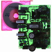
EVL6562A-35WFLB STMicroelectronics, EVL6562A-35WFLB Datasheet - Page 9

EVL6562A-35WFLB
Manufacturer Part Number
EVL6562A-35WFLB
Description
BOARD EVAL FOR L6562AX
Manufacturer
STMicroelectronics
Type
Power Factor Correctionr
Specifications of EVL6562A-35WFLB
Main Purpose
Power Management, Power Factor Correction
Embedded
No
Utilized Ic / Part
L6562A
Primary Attributes
35W, 48V Out, 90 ~ 265VAC In
Secondary Attributes
Transition Mode
Input Voltage
90 V to 265 V
Output Voltage
48 V
Board Size
120 mm x 82 mm
Product
Power Management Modules
Dimensions
120 mm x 82 mm
Lead Free Status / RoHS Status
Lead free / RoHS Compliant
For Use With/related Products
L6562A
Other names
497-8248
Available stocks
Company
Part Number
Manufacturer
Quantity
Price
Company:
Part Number:
EVL6562A-35WFLB
Manufacturer:
ON
Quantity:
100
Part Number:
EVL6562A-35WFLB
Manufacturer:
ST
Quantity:
20 000
L6562
When the load of a PFC pre-regulator is very low, the output voltage tends to stay steadily above the nom-
inal value, which cannot be handled by the Dynamic OVP. If this occurs, however, the error amplifier out-
put will saturate low; hence, when this is detected, the external power transistor is switched off and the IC
put in an idle state (Static OVP). Normal operation is resumed as the error amplifier goes back into its lin-
ear region. As a result, the L6562 will work in burst-mode, with a repetition rate that can be very low.
When either OVP is activated the quiescent consumption of the IC is reduced to minimize the discharge
of the Vcc capacitor and increase the hold-up capability of the IC supply system.
4.2 THD optimizer circuit
The L6562 is equipped with a special circuit that reduces the conduction dead-angle occurring to the AC
input current near the zero-crossings of the line voltage (crossover distortion). In this way the THD (Total
Harmonic Distortion) of the current is considerably reduced.
A major cause of this distortion is the inability of the system to transfer energy effectively when the instan-
taneous line voltage is very low. This effect is magnified by the high-frequency filter capacitor placed after
the bridge rectifier, which retains some residual voltage that causes the diodes of the bridge rectifier to be
reverse-biased and the input current flow to temporarily stop.
Figure 22. THD optimization: standard TM PFC controller (left side) and L6562 (right side)
Input current
Input current
Rectified mains voltage
Rectified mains voltage
Imains
Input current
Imains
Input current
Vdrain
MOSFET's drain voltage
Vdrain
MOSFET's drain voltage
To overcome this issue the circuit embedded in the L6562 forces the PFC pre-regulator to process more
energy near the line voltage zero-crossings as compared to that commanded by the control loop. This will
result in both minimizing the time interval where energy transfer is lacking and fully discharging the high-
frequency filter capacitor after the bridge. The effect of the circuit is shown in figure 23, where the key
waveforms of a standard TM PFC controller are compared to those of the L6562.
Essentially, the circuit artificially increases the ON-time of the power switch with a positive offset added to
9/16


