CDB3310 Cirrus Logic Inc, CDB3310 Datasheet - Page 9
CDB3310
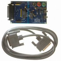
Manufacturer Part Number
CDB3310
Description
BOARD EVAL FOR CS3310 COL CTRL
Manufacturer
Cirrus Logic Inc
Datasheet
1.CS3310-KSZ.pdf
(17 pages)
Specifications of CDB3310
Main Purpose
Audio, Volume Control
Embedded
No
Utilized Ic / Part
CS3310
Primary Attributes
Stereo Volume Control, 0.5 dB Step Size, Serial Control
Secondary Attributes
-95.5 dB Attenuation, +31.5 dB Gain, 0.001% THD+N, 116 dB Dynamic Range
Product
Audio Modules
Lead Free Status / RoHS Status
Contains lead / RoHS non-compliant
Lead Free Status / RoHS Status
Lead free / RoHS Compliant, Contains lead / RoHS non-compliant
Other names
598-1000


CS3310
a source of distortion if the source impedance becomes appreciable relative to the reversed bi-
ased diode capacitance. Source impedances equal to or less than 600 ohms will avoid this dis-
tortion mechanism for the CS3310.
Mute
Muting can be achieved by either hardware or software control. Hardware muting is accom-
plished via the MUTE input and software muting by loading all zeroes into the volume control reg-
ister.
MUTE disconnects the internal buffer amplifiers from the output pins and terminates AOUTL and
AOUTR with 10 kΩ resistors to ground. The mute is activated with a zero crossing detection (in-
dependent of the zero cross enable status) or an 18 ms timeout to eliminate any audible “clicks”
or “pops”. MUTE also initiates an internal offset calibration.
A software mute is implemented by loading all zeroes into the volume control register. The inter-
nal amplifier is set to unity gain with the amplifier input connected to the maximum attenuation
point of the resistive divider, AGND.
A “soft mute” can be accomplished by sequentially ramping down from the current volume control
setting to the maximum attenuation code of all zeroes.
Power-Up Considerations
Upon initial application of power, the MUTE pin of the CS3310 should be set low to initiate a pow-
er-up sequence. This sequence sets the serial shift register and the volume control register to
zero and performs an offset calibration. The device should remain muted until the supply voltag-
es have settled to ensure an accurate calibration. The device also includes an internal power-on
reset circuit that requires approximately 100 µs to settle and will ignore any attempts to address
the internal registers during this period.
The offset calibration minimizes internally generated offsets and ignores offsets applied to the
AIN pins. External clocks are not required for calibration.
Although the device is tolerant to power supply variation, the device will enter a hardware mute
state if the power supply voltage drops below approximately ±3.5 volts. A power-up sequence
will be initiated if the power supply voltage returns to greater than ±3.5 volts.
Applying power to VD+ prior to VA+ creates a SCR latch-up condition. Refer to Figure 2 for the
recommended power connections.
DS82F1
9
Related parts for CDB3310
Image
Part Number
Description
Manufacturer
Datasheet
Request
R

Part Number:
Description:
Development Kit
Manufacturer:
Cirrus Logic Inc
Datasheet:
Part Number:
Description:
Development Kit
Manufacturer:
Cirrus Logic Inc
Datasheet:


Part Number:
Description:
High-efficiency PFC + Fluorescent Lamp Driver Reference Design
Manufacturer:
Cirrus Logic Inc
Datasheet:
Part Number:
Description:
Development Kit
Manufacturer:
Cirrus Logic Inc
Datasheet:
Part Number:
Description:
Development Kit
Manufacturer:
Cirrus Logic Inc
Datasheet:

Part Number:
Description:
Development Kit
Manufacturer:
Cirrus Logic Inc
Datasheet:
Part Number:
Description:
Development Kit
Manufacturer:
Cirrus Logic Inc
Datasheet:
Part Number:
Description:
Development Kit
Manufacturer:
Cirrus Logic Inc
Datasheet:
Part Number:
Description:
Development Kit
Manufacturer:
Cirrus Logic Inc
Datasheet:

Part Number:
Description:
EVALUATION BOARD FOR CS8427
Manufacturer:
Cirrus Logic Inc
Datasheet:

Part Number:
Description:
BOARD EVAL FOR CS8416 RCVR
Manufacturer:
Cirrus Logic Inc
Datasheet:

Part Number:
Description:
EVALUATION BOARD FOR CS8420
Manufacturer:
Cirrus Logic Inc
Datasheet:

Part Number:
Description:
KIT DEVELOPMENT EP9315 ARM9
Manufacturer:
Cirrus Logic Inc
Datasheet:

Part Number:
Description:
KIT DEVELOPMENT EP9302 ARM9
Manufacturer:
Cirrus Logic Inc
Datasheet: