MB88162EB01 Fujitsu Semiconductor America Inc, MB88162EB01 Datasheet
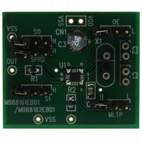
MB88162EB01
Specifications of MB88162EB01
Available stocks


Related parts for MB88162EB01


MB88162EB01 Summary of contents
Page 1
FUJITSU MICROELECTRONICS DATA SHEET Spread Spectrum Clock Generator MB88162 ■ DESCRIPTION MB88162 is a clock generator for EMI (Electro Magnetic Interference) reduction. The peak of unnecessary radiation noise (EMI) can be attenuated by making the oscillation frequency slightly modulate periodically ...
Page 2
MB88162 ■ PIN ASSIGNMENT ■ PIN DESCRIPTION Pin no. Pin name MLTP XIN 9 XOUT ...
Page 3
I/O CIRCUIT TYPE Pin 800 kΩ OE Note : At OE=“L” 22kΩ Pull Up cut S0, S1, SPRD Note : At OE=“L” Pull Up cut MLTP Note : At OE=“L” Pull Down cut OE signal OUT Note : At ...
Page 4
MB88162 (Continued) Pin XIN XIN, XOUT XOUT 4 Circuit type 4 pF 500 kΩ Remarks • Oscillation circuit • Built-in feedback resistance : 500 kΩ (Typ) • Built-in oscillation stabilization capacitance : 4 pF (Typ) ...
Page 5
HANDLING DEVICES Preventing Latch-up A latch-up can occur if, on this device, (a) a voltage higher than power supply voltage or a voltage lower than GND is applied to an input or output pin or (b) a voltage higher ...
Page 6
MB88162 ■ BLOCK DIAGRAM Output enable OE Multiplication rate setting MLTP Modulation type setting SPRD Modulation rate setting S0 Modulation rate setting XOUT XIN = 500 kΩ − Reference clock ...
Page 7
PIN SETTING After the pin setting is changed, the stabilization wait time of the modulation clock is required. The stabilization wait time of the modulation clock takes the maximum value of Lock-Up time in “• AC Characteristics” in ■ ...
Page 8
MB88162 • Center spread Spectrum is spread (modulated) by centering on the non-spread frequency. Radiation level Example of center spread modulation rate ± 1.0% • Down spread Spectrum is spread (modulated) below the non-spread frequency. Modulation width 2.0% Radiation level ...
Page 9
ABSOLUTE MAXIMUM RATINGS Parameter Power supply voltage* Input voltage* Output voltage* Storage temperature Operation junction temperature Output current Overshoot Undershoot = 0 The parameter is based WARNING: Semiconductor devices can be permanently damaged ...
Page 10
MB88162 ■ RECOMMENDED OPERATING CONDITIONS Parameter Symbol Power supply voltage V DD “H” level input voltage V IH “L” level input voltage V IL Input clock duty cycle t DCI Operating temperature Ta WARNING: The recommended operating conditions are required ...
Page 11
ELECTRICAL CHARACTERISTICS • DC Characteristics Parameter Symbol Power supply current I CC Power down current Output voltage V OL Output impedance Z OC Load capacitance C L Built-in oscillation C OSC stabilization capacitance R PUOEH ...
Page 12
MB88162 • AC Characteristics Parameter Symbol Input frequency f in Crystal oscillation f x frequency Output frequency f OUT Output clock rise time tr Output clock fall time tf Output clock duty cycle t DCC Modulation frequency f MOD Lock-Up ...
Page 13
OUTPUT CLOCK DUTY CYCLE (t × 0. OUT ■ INPUT FREQUENCY (f = 1/t in XIN ■ OUTPUT CLOCK RISE TIME/OUTPUT CLOCK FALL TIME (t OUT t r ■ CYCLE-CYCLE JITTER (t JC OUT Note : Cycle-cycle ...
Page 14
MB88162 ■ OUTPUT ENABLE “L” WIDTH (t OE ■ POWER SUPPLY RISE TIME ( ■ OUTPUT Hi-Z START TIME AFTER POWER DOWN ENTRY (t OE OUT ■ OUTPUT Hi-Z RELEASE TIME • OUTPUT START TIME AFTER POWER DOWN ...
Page 15
MODULATION WAVEFORM • Modulation rate ±1.0%, example of center spread OUT output frequency + 1.0 % Frequency at modulation OFF − 1.0 % • Modulation rate −2.0%, example of down spread OUT output frequency Frequency at modulation OFF − ...
Page 16
MB88162 ■ LOCK-UP TIME V DD XIN OE Setting pin S1, S0, MLTP SPRD OUT The clock oscillation stabilization wait time is required when the power is turned on. If the OE pin is fixed at “H” level, the maximum ...
Page 17
XIN Setting pin V IH S1, S0, MLTP (lock-up time ) SPRD OUT If the setting pin (S1, S0, MLTP, or SPRD) is used for control during normal operation, the required clock is obtained at most the ...
Page 18
MB88162 ■ CRYSTAL OSCILLATION CIRCUIT The figure below shows the connection example about general crystal resonator. The oscillation circuit has the built-in feedback resistor (500kΩ) and oscillation stabilization capacitance (4 pF) . Because the value of oscillation stabilization capacitance must ...
Page 19
ORDERING INFORMATION Part no. MB88162PVB-G-EFE1 MB88162PVB-G-ERE1 Package 18-pin plastic BCC (LCC-18P-M05) MB88162 Emboss taping EF type ER type 19 ...
Page 20
MB88162 ■ PACKAGE DIMENSION 18-pin plastic BCC (LCC-18P-M05) 2.70±0.10 (.106±.004 INDEX AREA (.094±.004 0.05(.002) 2003 FUJITSU LIMITED C18058S-c-1 0.45±0.05 (.018±.002) (Mount height) 2.01(.079) 2.40±0.10 TYP 0.45(.018) TYP. 0.075±0.025 (.003±.001) (Stand off) Details of "A" ...
Page 21
MEMO MB88162 21 ...
Page 22
MB88162 MEMO 22 ...
Page 23
MEMO MB88162 23 ...
Page 24
FUJITSU MICROELECTRONICS LIMITED Shinjuku Dai-Ichi Seimei Bldg. 7-1, Nishishinjuku 2-chome, Shinjuku-ku, Tokyo 163-0722, Japan Tel: +81-3-5322-3347 Fax: +81-3-5322-3387 http://jp.fujitsu.com/fml/en/ For further information please contact: North and South America FUJITSU MICROELECTRONICS AMERICA, INC. 1250 E. Arques Avenue, M/S 333 Sunnyvale, CA ...