ATAVRBC100 Atmel, ATAVRBC100 Datasheet - Page 9
ATAVRBC100
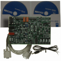
Manufacturer Part Number
ATAVRBC100
Description
REF DESIGN KIT BATTERY CHARGER
Manufacturer
Atmel
Series
AVR®r
Datasheet
1.ATAVRBC100.pdf
(12 pages)
Specifications of ATAVRBC100
Main Purpose
Power Management, Battery Charger
Embedded
Yes, MCU, 8-Bit
Utilized Ic / Part
ATtiny261/461/861/25/45/85
Primary Attributes
Multi Chemistry, 3 Circuits, (2) 1.2 ~ 20V @ 1A/2.5A Out, (1) 1.2 ~ 38V @ 5A
Secondary Attributes
7.5 ~ 40V In, 2 Relays, Supports Optional DB101 Display Board
Data Bus Width
8 bit
Interface Type
RS-232
Silicon Manufacturer
Atmel
Silicon Core Number
AVR451
Kit Application Type
Power Management - Battery
Application Sub Type
Battery Charger
Silicon Family Name
AVR
Rohs Compliant
Yes
Lead Free Status / RoHS Status
Lead free / RoHS Compliant


4.6 Jumpers overview
8088A-AVR-09/07
ATmega644 board controller it can be programmed regardless of the state of the SPI
lines. If SPI communication is used between a ATtiny and the ATmega644 a way to
ensure that programming is successful, is to erase the ATmega644 first, next
program the ATtiny and finally program the ATmega644.
During development the JTAG and DebugWire debugging interfaces are used, these
are not using the SPI lines to program the devices, and there are thus no special
procedures that should be followed to ensure successful programming.
In general the ATtinyx5 and the ATtinyx61 sockets should not be populated at the
same time, as the devices in these sockets are connected to the same traces on the
BC100. If devices are placed in both of these sockets it could potentially result in
drive contention.
A number of jumpers are available on the BC100, to be able to configure it for the
desired use. Please refer to Table 4-2 for a list of jumper and use, and refer to Figure
4-2 to identify the jumper’s location.
Table 4-2. Jumper and their use.
Designator
J302
J400/401
J402
J403
J404
J405
J406
Use and settings
Selects if the PB1 pin on ATtinyx5 is connected to the ISP/dW header or if
it is connected to the buck converters.
Use “PROG” position (left on Figure 4-2) when programming the
ATtinyx5.
Use “CHARGE” position when the ATtinyx5 should be connected to a
buck burst converter.
Select which buck converter the supply voltage is connected to use.
Two jumpers should be mounted in side by side at the label “BUCK-A”
(40V/5A), BUCK-B” (30V/2.5A) or BUCK-C” (20V/1A). “BUCK-A is the
rightmost jumper pair on Figure 4-2
Selects if the buck PWM control signal is connected or disconnected from
the BUCK-A (40V/5A). This jumper should be mounted in the disable
position while J403 or J404 is mounted in the enable position.
Selects if the buck PWM control signal is connected or disconnected from
the BUCK-B (30V/2.5A). This jumper should be mounted in the disable
position while J402 or J404 is mounted in the enable position.
Selects if the buck PWM control signal is connected or disconnected from
the BUCK-C (20V/1A). This jumper should be mounted in the disable
position while J402 or J403 is mounted in the enable position.
Selects the resistor divider network setting for the ADC input from the
V_BAT+ voltage (positive ADC input from shunt resistor).
The divider can be set to 1/2, 1/4, 1/8, 1/12, and 1/16 V_BAT+.
Note that the setting used should match the setting on J406.
Selects the resistor divider network setting for the ADC input from the
V_BAT- voltage (negative ADC input from shunt resistor).
The divider can be set to 1/2, 1/4, 1/8, 1/12, and 1/16 V_BAT-.
Note that the setting used should match the setting on J405.
AVR451
9
Related parts for ATAVRBC100
Image
Part Number
Description
Manufacturer
Datasheet
Request
R

Part Number:
Description:
DEV KIT FOR AVR/AVR32
Manufacturer:
Atmel
Datasheet:

Part Number:
Description:
INTERVAL AND WIPE/WASH WIPER CONTROL IC WITH DELAY
Manufacturer:
ATMEL Corporation
Datasheet:
Part Number:
Description:
Low-Voltage Voice-Switched IC for Hands-Free Operation
Manufacturer:
ATMEL Corporation
Datasheet:
Part Number:
Description:
MONOLITHIC INTEGRATED FEATUREPHONE CIRCUIT
Manufacturer:
ATMEL Corporation
Datasheet:
Part Number:
Description:
AM-FM Receiver IC U4255BM-M
Manufacturer:
ATMEL Corporation
Datasheet:
Part Number:
Description:
Monolithic Integrated Feature Phone Circuit
Manufacturer:
ATMEL Corporation
Datasheet:
Part Number:
Description:
Multistandard Video-IF and Quasi Parallel Sound Processing
Manufacturer:
ATMEL Corporation
Datasheet:
Part Number:
Description:
High-performance EE PLD
Manufacturer:
ATMEL Corporation
Datasheet:
Part Number:
Description:
8-bit Flash Microcontroller
Manufacturer:
ATMEL Corporation
Datasheet:
Part Number:
Description:
2-Wire Serial EEPROM
Manufacturer:
ATMEL Corporation
Datasheet: