DV250501 Microchip Technology, DV250501 Datasheet - Page 13
DV250501
Manufacturer Part Number
DV250501
Description
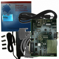
KIT DEV CAN MCP250XX
Manufacturer
Microchip Technology
Type
Network Controller & Processorr
Specifications of DV250501
Main Purpose
Interface, CAN I/O Expander
Embedded
Yes, MCU, 8-Bit
Utilized Ic / Part
MCP25020, MCP25050
Primary Attributes
V2.0B up to 1Mb/s Data Rate
Data Rate
1 Mbps
Interface Type
CAN
Operating Voltage
2.7 V to 5.5 V
Product
Modules
Lead Free Status / RoHS Status
Lead free / RoHS Compliant
Secondary Attributes
-
Lead Free Status / Rohs Status
Lead free / RoHS Compliant
Other names
Q1221418
Available stocks
Company
Part Number
Manufacturer
Quantity
Price
Company:

Part Number:
DV250501
Manufacturer:
MICROCHIP
Quantity:
12 000
Part Number:
DV250501
Manufacturer:
MICROCHIP/微芯
Quantity:
20 000


2004 Microchip Technology Inc.
1.5.4
The Device Programmer module is used with PC software to configure the
user-defined defaults.
FIGURE 1-4:
1.5.5
There are a few key areas on the board. Figure 1-4 illustrates these areas, while
Table 1-1 details them.
TABLE 1-1:
D2, D3, D4 and D5 CAN traffic indicator LEDs. D2 represents all traffic. D3-D5 represent
U11, U12, U13, J3
U15, J5 and JP4
Y1, Y2, Y3, JP1
Key Areas
and JP2
and J4
DB25
U14
U6
U3
Device Programmer
Key Areas of the MCP2515
J5
MCP250XX BOARD LAYOUT
U15
U6
DB25 is the connection to the host PC interface. The PC controls both
the PC Node and the Device Programmer circuit.
U6 is the CAN Controller (MCP2515) of the PC Node that is controlled
by the host PC.
U15 is the prototyping node. J5 is the ICSP™ header for U15. JP4 jump-
ers board power to the V
J5 (ICSP header) to isolate U15 from the rest of the board during
In-Circuit Serial Programming™.
The MCP250XX for the demonstration program. Connected to the
potentiometers, piezo, buttons and lamp.
U3 is the socket for programming the user-defined defaults using the
programming software.
Y1, Y2 and Y3 are the oscillator sockets for each of the three CAN
nodes. By default, all of the Yx outputs are connected together (JP1 and
JP2 are shorted via a trace on the back of the board) and only Y1 is pop-
ulated (i.e., Y1 clocks all three CAN nodes). To separate the oscillator
sockets, the traces shorting JP1 and JP2 must be cut.
U11-U13 are the CAN drivers all connected to a common CAN bus. The
two DB9s (J3 and J4) are the external CAN bus connections. Only J4 is
populated.
transmitted traffic of each of the three nodes.
MCP250XX DEVELOPMENT BOARD
NODE A
DB25
PC NODE
Y1
Y2
J1
Y3
DD
D2
D3
D4
D5
BZ1
J4
pin of U15 and should be removed if using
Description
R17
100
U3
GP4
DEVICE PROGRAMMER
R20
100
NODE B
GP5 GP6
U2
U14
S1
J3
L1
DS51266C-page 9
Related parts for DV250501
Image
Part Number
Description
Manufacturer
Datasheet
Request
R

Part Number:
Description:
Manufacturer:
Microchip Technology Inc.
Datasheet:
Part Number:
Description:
Manufacturer:
Microchip Technology Inc.
Datasheet:
Part Number:
Description:
Manufacturer:
Microchip Technology Inc.
Datasheet:
Part Number:
Description:
Manufacturer:
Microchip Technology Inc.
Datasheet:
Part Number:
Description:
Manufacturer:
Microchip Technology Inc.
Datasheet:
Part Number:
Description:
Manufacturer:
Microchip Technology Inc.
Datasheet:
Part Number:
Description:
Manufacturer:
Microchip Technology Inc.
Datasheet:
Part Number:
Description:
Manufacturer:
Microchip Technology Inc.
Datasheet: