MCP6XXXDM-FLTR Microchip Technology, MCP6XXXDM-FLTR Datasheet - Page 35
MCP6XXXDM-FLTR
Manufacturer Part Number
MCP6XXXDM-FLTR
Description
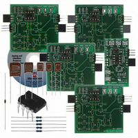
KIT DEMO BOARD ACTIVE FILTER
Manufacturer
Microchip Technology
Datasheet
1.MCP6XXXDM-FLTR.pdf
(46 pages)
Specifications of MCP6XXXDM-FLTR
Main Purpose
Filters, Active - Bandpass, Highpass, Lowpass
Embedded
Yes, MCU, 8-Bit
Utilized Ic / Part
MCP6271
Primary Attributes
Cascadable PCBs, Single Supply
Secondary Attributes
Bessel, Butterworth, and Chebyshev, with Order 1 ~ 8
Processor To Be Evaluated
MCP6271
Lead Free Status / RoHS Status
Not applicable / Not applicable
Lead Free Status / RoHS Status
Lead free / RoHS Compliant, Not applicable / Not applicable
Available stocks
Company
Part Number
Manufacturer
Quantity
Price
Company:

Part Number:
MCP6XXXDM-FLTR
Manufacturer:
MICROCHIP
Quantity:
12 000
Part Number:
MCP6XXXDM-FLTR
Manufacturer:
MICROCHIP/微芯
Quantity:
20 000


A.1
A.2
© 2006 Microchip Technology Inc.
INTRODUCTION
V
DD
/2 FILTER SECTION (SUB-ASSEMBLY #: 102-00098R1)
This appendix contains the schematics and layouts for the different pieces of the Active
Filter Demo Board Kit Sub-assemblies:
• V
• Active Filter Section (Sub-Assembly # : 102-00097R1)
• Accessory Bag (Sub-Assembly # : 110-00097R1)
A.2.1
See Figure A-1 for the V
headers (J1, J2, P1, and P2) allow the PCBs to be cascaded as needed. The filter order
will determine how many of the Active Filter Section boards need to be cascaded.
R1, R2, and C3 produce a V
reference voltage, and is set to unity gain. U1 must drive the impedances connected to
it on all of the Active Filter Section. Op amp U1 is usually a single, PDIP-8 part inserted
into the DIP-8 socket; it can be a SOIC-8 that is soldered to the board (see U1A in
Figure A-1).
C1 and C2 are bypass capacitors for V
The demonstration board includes five test points for convenience on the bench. TP1
and TP2 make it possible to connect a function generator to the filter input; this signal
is passed on to the other boards. TP3 through TP5 provide connections for external
power supplies, which are also passed on to the other boards.
JP1 allows the user to choose the V
• A lab supply (EXT = External V
• Op amp U1’s output (INT = Internal V
See Section B.1 “V
Appendix A. Schematics and Layouts
DD
/2 Filter Section (Sub-Assembly # : 102-00098R1)
Circuit
ACTIVE FILTER DEMO BOARD KIT
DD
/2 Filter Section BOMs” for the Bill of Material for this kit.
DD
/2 Filter Section circuit diagram. The input and output
DD
/2 reference voltage. The op amp U1 buffers this
DD
/2 source)
DD
/2 reference voltage source:
DD
DD
.
/2 source)
USER’S GUIDE
DS51614A-page 31
Related parts for MCP6XXXDM-FLTR
Image
Part Number
Description
Manufacturer
Datasheet
Request
R

Part Number:
Description:
Manufacturer:
Microchip Technology Inc.
Datasheet:
Part Number:
Description:
Manufacturer:
Microchip Technology Inc.
Datasheet:
Part Number:
Description:
Manufacturer:
Microchip Technology Inc.
Datasheet:
Part Number:
Description:
Manufacturer:
Microchip Technology Inc.
Datasheet:
Part Number:
Description:
Manufacturer:
Microchip Technology Inc.
Datasheet:
Part Number:
Description:
Manufacturer:
Microchip Technology Inc.
Datasheet:
Part Number:
Description:
Manufacturer:
Microchip Technology Inc.
Datasheet:
Part Number:
Description:
Manufacturer:
Microchip Technology Inc.
Datasheet: