YNV12T16-0G POWER ONE, YNV12T16-0G Datasheet - Page 8
YNV12T16-0G
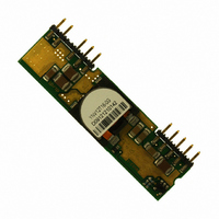
Manufacturer Part Number
YNV12T16-0G
Description
CONVERTER DC-DC 12V 16A SIP
Manufacturer
POWER ONE
Series
Yr
Type
Point of Load (POL) Non-Isolatedr
Datasheet
1.YNV12T16-0G.pdf
(28 pages)
Specifications of YNV12T16-0G
Output
0.75 ~ 5.5V
Number Of Outputs
1
Power (watts)
88W
Mounting Type
Through Hole
Voltage - Input
9.6 ~ 14V
Package / Case
10-SIP Module
1st Output
0.75 ~ 5.5 VDC @ 16A
Size / Dimension
2.00" L x 0.28" W x 0.54" H (50.8mm x 7.1mm x 13.7mm)
Power (watts) - Rated
88W
Operating Temperature
-40°C ~ 85°C
Efficiency
94%
Approvals
cUL, EN, UL
Package
10SIP
Output Current
16 A
Output Voltage
0.7525 to 5.5 V
Input Voltage
12 V
Output Power
88 W
Switching Regulator
Yes
Product
Non-Isolated / POL
Input Voltage Range
9.6 V to 14 V
Input Voltage (nominal)
12 V
Output Voltage (channel 1)
0.7525 V to 5.5 V
Output Current (channel 1)
16 A
Package / Case Size
SIP
Output Type
Regulated
Lead Free Status / RoHS Status
Lead free / RoHS Compliant
3rd Output
-
2nd Output
-
Lead Free Status / Rohs Status
Lead free / RoHS Compliant
Other names
179-2378


Characterization
General Information
The converter has been characterized for many
operational aspects, to include thermal derating
(maximum load current as a function of ambient
temperature and airflow) for vertical mounting,
efficiency, start-up and shutdown parameters,
output ripple and noise, transient response to load
step-change, overload and short circuit.
The figures are numbered as Fig. x.y, where x
indicates the different output voltages, and y
associates with specific plots (y = 1 for the vertical
thermal derating, …). For example, Fig. x.1 will
refer to the vertical thermal derating for all the
output voltages in general.
The following pages contain specific plots or
waveforms
Additional comments for specific data are provided
below.
Test Conditions
All thermal and efficiency data presented were
taken with the converter soldered to a test board,
specifically a 0.060” thick printed wiring board
(PWB) with four layers. The top and bottom layers
were not metalized. The two inner layers,
comprising two-ounce copper, were used to
provide traces for connectivity to the converter.
The lack of metalization on the outer layers as well
as the limited thermal connection ensured that
heat transfer from the converter to the PWB was
minimized. This provides a worst-case but
consistent scenario for thermal derating purposes.
All measurements requiring airflow were made in
vertical and horizontal wind tunnel facilities using
Infrared (IR) thermography and thermocouples for
thermometry.
Ensuring components on the converter do not
exceed their ratings is important to maintaining
high reliability. If one anticipates operating the
converter at or close to the maximum loads
specified in the derating curves, it is prudent to
check actual operating temperatures in the
application. Thermographic imaging is preferable;
if
thermocouples
recommends the use of AWG #40 gauge
thermocouples to ensure measurement accuracy.
ZD-02039 Rev. 3.2, 24-Jun-10
this
capability
associated
may
is
be
9.6-14 VDC Input; 0.7525-5.5 VDC Programmable @ 16A
with
not
used.
available,
the
Power-One
converter.
then
YNV12T16 DC-DC Converter Data Sheet
Page 8 of 28
Careful routing of the thermocouple leads will
further minimize measurement error. Refer to Fig.
D for optimum measuring thermocouple location.
Thermal Derating
Load current vs. ambient temperature and airflow
rates are given in Figs. x.1 for maximum
temperature of 120 °C. Ambient temperature was
varied between 25 °C and 85 °C, with airflow rates
from 30 to 500 LFM (0.15 m/s to 2.5 m/s), and
vertical converter mounting. The airflow during the
testing is parallel to the long axis of the converter,
going from input pins to output pins.
For each set of conditions, the maximum load
current was defined as the lowest of:
(i) The output current at which any MOSFET
temperature
specified temperature (120 °C) as indicated by the
thermographic image, or
(ii) The maximum current rating of the converter
(16 A)
During normal operation, derating curves with
maximum FET temperature less than or equal to
120 °C should not be exceeded. Temperature on
the PCB at the thermocouple location shown in
Fig. D should not exceed 120 °C in order to
operate inside the derating curves.
Fig. D: Location of the thermocouple for thermal testing.
www.power-one.com
does
not
exceed
a
maximum
Related parts for YNV12T16-0G
Image
Part Number
Description
Manufacturer
Datasheet
Request
R

Part Number:
Description:
SWITCHING POWER SUPPLIES, SINGLE OUTPUT, 80 WATTS
Manufacturer:
POWER ONE
Datasheet:
Part Number:
Description:
HAS SERIES - 30 WATT
Manufacturer:
POWER ONE
Datasheet:
Part Number:
Description:
SINGLE OUTPUT
Manufacturer:
POWER ONE
Datasheet:

Part Number:
Description:
BRS DC/DC converters(1.5 WATT)
Manufacturer:
Power-One
Datasheet:
Part Number:
Description:
3...15 Watt DC-DC Converter
Manufacturer:
Power-One
Datasheet:
Part Number:
Description:
HBS SERIES - 100 WATT
Manufacturer:
Power-One
Datasheet:
Part Number:
Description:
3...15 Watt DC-DC Converter
Manufacturer:
Power-One
Datasheet:
Part Number:
Description:
BUS DC/DC converters(3 WATT)
Manufacturer:
Power-One
Datasheet:
Part Number:
Description:
HES SERIES 150 WATT
Manufacturer:
Power-One
Datasheet:
Part Number:
Description:
1.25 WATT
Manufacturer:
Power-One
Datasheet: