LTM4600HVMPV#PBF Linear Technology, LTM4600HVMPV#PBF Datasheet - Page 6
LTM4600HVMPV#PBF
Manufacturer Part Number
LTM4600HVMPV#PBF
Description
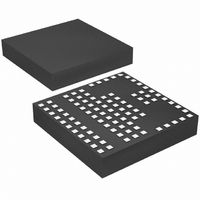
IC DC/DC UMODULE 10A 104-LGA
Manufacturer
Linear Technology
Series
µModuler
Type
Point of Load (POL) Non-Isolatedr
Datasheet
1.LTM4600HVEVPBF.pdf
(24 pages)
Specifications of LTM4600HVMPV#PBF
Output
0.6 ~ 5 V
Number Of Outputs
1
Power (watts)
50W
Mounting Type
Surface Mount
Voltage - Input
4.5 ~ 28 V
Package / Case
104-LGA
1st Output
0.6 ~ 5 VDC @ 10A
Size / Dimension
0.59" L x 0.59" W x 0.11" H (15mm x 15mm x 2.8mm)
Power (watts) - Rated
50W
Operating Temperature
-55°C ~ 125°C
Efficiency
92%
Lead Free Status / RoHS Status
Lead free / RoHS Compliant
3rd Output
-
2nd Output
-
Available stocks
Company
Part Number
Manufacturer
Quantity
Price


PI FU CTIO S
LTM4600HV
V
between these pins and GND pins. Recommend placing
input decoupling capacitance directly between V
and GND pins.
f
the one-shot timer current, thereby setting the switching
frequency. The LTM4600HV switching frequency is typically
850kHz. An external resistor to ground can be selected to
reduce the one-shot timer current, thus lower the switching
frequency to accommodate a higher duty cycle step down
requirement. See the applications section.
SV
this pin open or add additional decoupling capacitance.
EXTV
left open or grounded, the internal 5V linear regulator will
power the controller and MOSFET drivers. For high input
voltage applications, connecting this pin to an external
5V will reduce the power loss in the power module. The
EXTV
V
Internally, this pin is connected to V
resistor. Different output voltages can be programmed with
additional resistors between the V
COMP (Pin B23): Current Control Threshold and Error
Amplifi er Compensation Point. The current comparator
threshold increases with this control voltage. The voltage
ranges from 0V to 2.4V with 0.8V corresponding to zero
sense voltage (zero current).
6
ADJ
OSET
IN
IN
U
(Bank 1): Power Input Pins. Apply input voltage
(Pin A15): A 110k resistor from V
(Pin A17): Supply Pin for Internal PWM Controller. Leave
CC
CC
(Pin A21): The Negative Input of The Error Amplifi er.
(Pin A19): External 5V supply pin for controller. If
voltage should never be higher than V
U
U
(See Package Description for Pin Assignment)
OUT
OSET
BANK 1
BANK 2
BANK 3
with a 100k precision
PGND
V
OUT
V
and SGND pins.
IN
IN
to this pin sets
1 2
2 5
3 2
8
1
1
3 9
5 0
6 1
7 2
8 3
9 4
2
3
2
4 0
5 1
6 2
7 3
8 4
9 5
4
IN
3
5
.
4 1
5 2
6 3
7 4
8 5
9 6
6
IN
2 6
3 3
7
4
9 7
4 2
5 3
6 4
7 5
8 6
8
pins
2 7
3 4
9
5
10
1 3
4 3
5 4
6 5
7 6
8 7
9 8
9
TOP VIEW
11
2 8
3 5
6
12
1 0
1 4
4 4
5 5
6 6
7 7
8 8
9 9
13
2 9
3 6
7
14
1 0 0
1 1
1 5
4 5
5 6
6 7
7 8
8 9
SGND (Pin D23): Signal Ground Pin. All small-signal
components should connect to this ground, which in turn
connects to PGND at one point.
RUN/SS (Pin F23): Run and Soft-Start Control. Forcing
this pin below 0.8V will shut down the power supply.
Inside the power module, there is a 1000pF capacitor
which provides approximately 0.7ms soft-start time with
200μF output capacitance. Additional soft-start time can
be achieved by adding additional capacitance between
the RUN/SS and SGND pins. The internal short-circuit
latchoff can be disabled by adding a resistor between this
pin and the V
5μA pull up current.
FCB (Pin G23): Forced Continuous Input. Grounding this
pin enables forced continuous mode operation regardless
of load conditions. Tying this pin above 0.63V enables
discontinuous conduction mode to achieve high effi ciency
operation at light loads. There is an internal 4.75K resistor
between the FCB and SGND pins.
PGOOD (Pin J23): Output Voltage Power Good Indicator.
When the output voltage is within 10% of the nominal
voltage, the PGOOD is open drain output. Otherwise, this
pin is pulled to ground.
PGND (Bank 2): Power ground pins for both input and
output returns.
V
between these pins and GND pins. Recommend placing
High Frequency output decoupling capacitance directly
between these pins and GND pins.
1 6
3 0
3 7
15
OUT
1 0 1
4 6
5 7
6 8
7 9
9 0
16
1 7
3 1
3 8
17
1 0 2
18
4 7
5 8
6 9
8 0
9 1
(Bank 3): Power Output Pins. Apply output load
19
1 8
1 0 3
20
4 8
5 9
7 0
8 1
9 2
1 9
21
1 0 4
4 9
6 0
7 1
8 2
9 3
22
23
2 0
2 1
2 2
2 3
2 4
IN
A
C
E
G
J
L
M
N
P
R
T
pin. This resistor must supply a minimum
B
D
F
H
K
4600hv PN01
COMP
SGND
RUN/SS
FCB
PGOOD
4600hvfc
Related parts for LTM4600HVMPV#PBF
Image
Part Number
Description
Manufacturer
Datasheet
Request
R

Part Number:
Description:
10a, 28vin High Efficiency Dc/dc ?module
Manufacturer:
Linear Technology Corporation
Datasheet:

Part Number:
Description:
IC DC/DC UMODULE 10A 104-LGA
Manufacturer:
Linear Technology
Datasheet:
Part Number:
Description:
IC DC/DC UMODULE 10A 104-LGA
Manufacturer:
Linear Technology
Datasheet:

Part Number:
Description:
10A High Effi ciency DC/DC ?Module
Manufacturer:
LINER [Linear Technology]
Datasheet:

Part Number:
Description:
IC DC/DC UMODULE 10A 104-LGA
Manufacturer:
Linear Technology
Datasheet:
Part Number:
Description:
IC DC/DC UMODULE 10A 104-LGA
Manufacturer:
Linear Technology
Datasheet:

Part Number:
Description:
CD ROM LINEARVIEW DATASHEETS
Manufacturer:
Linear Technology
Part Number:
Description:
Standalone Linear Li-Ion Battery Charger with Thermal Regulation in ThinSOT
Manufacturer:
Linear Technology Corporation
Datasheet:
Part Number:
Description:
Low noise, high frequency, 8th order linear phase lowpass filter
Manufacturer:
Linear Technology Corporation
Datasheet:
Part Number:
Description:
Manufacturer:
Linear Technology Corporation
Datasheet:
Part Number:
Description:
Manufacturer:
Linear Technology Corporation
Datasheet:
Part Number:
Description:
Manufacturer:
Linear Technology Corporation
Datasheet:
Part Number:
Description:
Manufacturer:
Linear Technology Corporation
Datasheet:
Part Number:
Description:
Manufacturer:
Linear Technology Corporation
Datasheet:
Part Number:
Description:
Manufacturer:
Linear Technology Corporation
Datasheet: