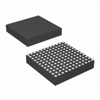
LTM4616EV#PBF Linear Technology, LTM4616EV#PBF Datasheet - Page 6

LTM4616EV#PBF
Manufacturer Part Number
LTM4616EV#PBF
Description
IC DC/DC UMODULE DUAL 8A 144-LGA
Manufacturer
Linear Technology
Series
µModuler
Type
Point of Load (POL) Non-Isolatedr
Datasheet
1.LTM4616EVPBF.pdf
(28 pages)
Specifications of LTM4616EV#PBF
Design Resources
LTM4616 Spice Model
Output
0.6 ~ 5 V
Number Of Outputs
2
Power (watts)
12W
Mounting Type
Surface Mount
Voltage - Input
2.7 ~ 5.5 V
Package / Case
144-LGA
1st Output
0.6 ~ 5 VDC @ 8A
2nd Output
0.6 ~ 5 VDC @ 8A
Size / Dimension
0.59" L x 0.59" W x 0.11" H (15mm x 15mm x 2.8mm)
Power (watts) - Rated
12W
Operating Temperature
-40°C ~ 125°C
Lead Free Status / RoHS Status
Lead free / RoHS Compliant
3rd Output
-
Available stocks
Company
Part Number
Manufacturer
Quantity
Price
LTM4616
typical perForMance characteristics
pin Functions
V
D1-D2) and (J1-J2, K1-K2, L1-L4, M1-M4): Power Input
Pins. Apply input voltage between these pins and GND
pins. Recommend placing input decoupling capacitance
directly between V
V
F9-F12) and (K9-K12, L9-L12, M9-M12): Power Output
Pins. Apply output load between these pins and GND
pins. Recommend placing output decoupling capacitance
directly between these pins and GND pins. See Table 1.
6
0.5V/DIV
IN1
OUT1
2V/DIV
V
3.0
2.5
2.0
1.5
1.0
0.5
OUT
V
, V
0
IN
, V
0
Start-Up
2.5V Output Current
V
V
C
(DEFAULT 100µs SOFT-START)
IN2
IN
OUT
OUT
= 5V
OUT2
, (BANK1 and BANK2); (F1-F4, E1-E4, C1-C2,
= 1.5V
= 100µF NO LOAD AND 8A LOAD
5
OUTPUT CURRENT (A)
(BANK3 and BANK6); (D9-D12, E9-E12,
IN
50µs/DIV
10
pins and GND pins.
15
4616 G16
4616 G13
20
2V/DIV
2V/DIV
5A/DIV
594
602
600
598
596
592
590
–50
V
Short-Circuit Protection
(2.5V Short, No Load)
V
V
IN
OUT
FB
= 5V
–25
vs Temperature
= 2.5V
V
V
I
OUT
IN
OUT
0
TEMPERATURE (°C)
25
50µs/DIV
GND1 and GND2 (BANK2 and BANK5); (A1-A5, A12, B1-
B5, B7-B12, C3-C12, D3-D7) and (G1-G5, G12, H1-H5,
H7-H12, J3-J12, K3-K7): Power Ground Pins for Both
Input and Output Returns.
SV
Channel. This pin is internally connected to V
a lowpass filter.
SGND1 and SGND2 (F5 and M5): Signal Ground Pin for
Each Channel. Return ground path for all analog and low
power circuitry. Tie a single connection to the output
capacitor GND in the application. See layout guidelines
in Figure 17.
50
IN1
V
V
V
IN
IN
IN
and SV
75
= 5.5V
= 3.3V
= 2.7V
100
Specified as Each Channel
4616 G17
4616 G14
IN2
125
(E5 and L5): Signal Input Voltage for Each
5V/DIV
5V/DIV
5A/DIV
–0.6
–0.1
–0.2
–0.3
–0.4
–0.5
0
0
Load Regulation vs Current
Short-Circuit Protection
(2.5V Short, 4A Load)
V
V
FC MODE
V
V
IN
OUT
IN
OUT
= 5V
V
V
= 3.3V
IN
OUT
= 2.5V
= 1.5V
2
LOAD CURRENT (A)
50µs/DIV
4
IN
I
6
OUT
through
LOAD
4616 G18
4616fc
4616 G15
8


