AFBR-5805AZ Avago Technologies US Inc., AFBR-5805AZ Datasheet - Page 6
AFBR-5805AZ
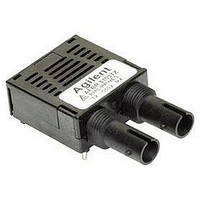
Manufacturer Part Number
AFBR-5805AZ
Description
TXRX ATM SONET OC3 3V SC 1X9
Manufacturer
Avago Technologies US Inc.
Datasheet
1.AFBR-5805TZ.pdf
(14 pages)
Specifications of AFBR-5805AZ
Applications
General Purpose
Wavelength
1310nm
Voltage - Supply
3.3V
Connector Type
SC
Mounting Type
Through Hole
Data Rate Max
0.1Gbps
Supply Voltage
5V
Wavelength Typ
1300nm
Leaded Process Compatible
Yes
Optical Fiber Type
TX/RX
Data Transfer Rate
100Mbps
Optical Rise Time
3/2.2ns
Optical Fall Time
3/2.2ns
Jitter
1.2/1.91ns
Operating Temperature Classification
Commercial
Peak Wavelength
1380nm
Operating Supply Voltage (min)
3.135/4.75V
Operating Supply Voltage (typ)
3.3/5V
Operating Supply Voltage (max)
3.5/5.25V
Output Current
50mA
Operating Temp Range
-10C to 85C
Mounting
Through Hole
Pin Count
9
Lead Free Status / RoHS Status
Lead free / RoHS Compliant
Data Rate
-
Lead Free Status / Rohs Status
Compliant


Transceiver Signaling Operating Rate Range and BER Per-
formance
For purposes of definition, the symbol (Baud) rate, also
called signaling rate, is the reciprocal of the symbol time.
Data rate (bits/sec) is the symbol rate divided by the en-
coding factor used to encode the data (symbols/bit).
When used in 155 Mb/s SONET OC-3 applications the
performance of the 1300 nm transceivers, AFBR-5805 is
guaranteed to the full conditions listed in product speci-
fication tables.
The transceivers may be used for other applications at
signaling rates different than 155 Mb/s with some varia-
tion in the link optical power budget. Figure 5 gives an
indication of the typical performance of these products
at different rates.
These transceivers can also be used for applications
which require different Bit Error Rate (BER) performance.
Figure 6 illustrates the typical trade-off between link BER
and the receivers input optical power level.
Figure 5. Transceiver Relative Optical Power Budget at Constant
BER vs. Signaling Rate.
2.5
2.0
1.5
1.0
0.5
0.5
0
0
CONDITIONS:
1. PRBS 2
2. DATA SAMPLED AT CENTER OF DATA SYMBOL.
3. BER = 10
4. T
5. V
6. INPUT OPTICAL RISE/FALL TIMES = 1.0/2.1 ns.
A
CC
25
= +25˚ C
= 3.3 V to 5 V dc
7
-1
50
-6
SIGNAL RATE (MBd)
75
100
125
150
175
200
Figure 6. Bit Error Rate vs. Relative Receiver Input Optical Power.
Transceiver Jitter Performance
The Avago Technologies 1300 nm transceivers are de-
signed to operate per the system jitter allocations stated
in Table B1 of Annex B of the draft ANSI T1E1.2 Revision
3 standard.
The Avago Technologies 1300 nm transmitters will
tolerate the worst case input electrical jitter allowed in
Annex B without violating the worst case output jitter
requirements.
The Avago Technologies 1300 nm receivers will tolerate
the worst case input optical jitter allowed in Annex B
without violating the worst case output electrical jitter
allowed.
The jitter specifications stated in the following 1300 nm
transceiver specification tables are derived from the
values in Tables B1 of Annex B. They represent the worst
case jitter contribution that the transceivers are allowed
to make to the overall system jitter without violating
the Annex B allocation example. In practice the typical
contribution of the Avago Technologies transceivers is
well below these maximum allowed amounts.
1 x 10⁻¹⁰
1 x 10-11
1 x 10-12
1 x 10⁻²
1 x 10⁻³
1 x 10⁻⁴
1 x 10⁻⁵
1 x 10⁻⁶
1 x 10⁻⁷
1 x 10⁻⁸
1 x 10⁻⁹
-6
CONDITIONS:
1. 155 MBd
2. PRBS 2
3. CENTER OF SYMBOL SAMPLING
4. T
5. V
6. INPUT OPTICAL RISE/FALL TIMES = 1.0/2.1 ns.
RELATIVE INPUT OPTICAL POWER - dB
A
CC
= +25˚C
= 3.3 V to 5 V dc
-4
7
-1
-2
AFBR-5805Z SERIES
CENTER OF SYMBOL
0
2
4
Related parts for AFBR-5805AZ
Image
Part Number
Description
Manufacturer
Datasheet
Request
R

Part Number:
Description:
650nm FE Transceiver Eval Kit
Manufacturer:
Avago Technologies US Inc.
Datasheet:

Part Number:
Description:
TXRX OPT OC3 MTRJ SFF 2X5DIP
Manufacturer:
Avago Technologies US Inc.
Datasheet:

Part Number:
Description:
TXRX ETHERNET 125MBD MMF 2X5
Manufacturer:
Avago Technologies US Inc.
Datasheet:

Part Number:
Description:
TXRX OPT SFP DGTL 850NM IND
Manufacturer:
Avago Technologies US Inc.
Datasheet:

Part Number:
Description:
TXRX OPT SFF 4/2/1GBD 2X7
Manufacturer:
Avago Technologies US Inc.
Datasheet:

Part Number:
Description:
TXRX OPT SFP 4/2/1GBD 850NM
Manufacturer:
Avago Technologies US Inc.
Datasheet:

Part Number:
Description:
TXRX OPT XFP 10GB/S 850NM
Manufacturer:
Avago Technologies US Inc.
Datasheet:

Part Number:
Description:
TXRX OPT 1X9 100MBPS ST EXT TEMP
Manufacturer:
Avago Technologies US Inc.
Datasheet:

Part Number:
Description:
TXRX OPT 1X9 100MBPS SC EXT TEMP
Manufacturer:
Avago Technologies US Inc.
Datasheet:

Part Number:
Description:
TXRX OPT 1X9 100MBPS DUPLEX SC
Manufacturer:
Avago Technologies US Inc.
Datasheet:

Part Number:
Description:
OPTOCOUPLER GATE DRV 2A 16-SOIC
Manufacturer:
Avago Technologies US Inc.
Datasheet:
Part Number:
Description:
OPTOCOUPLER 2CH 2.5A 16-SOIC
Manufacturer:
Avago Technologies US Inc.
Datasheet:

Part Number:
Description:
OPTOCOUPLER GATE DRV 0.4A 16SOIC
Manufacturer:
Avago Technologies US Inc.
Datasheet:

Part Number:
Description:
OPTOCOUPLER 2.0A 250KHZ 8-DIP
Manufacturer:
Avago Technologies US Inc.
Datasheet:

Part Number:
Description:
OPTOCOUPLER 2.0A 250KHZ GW 8-SMD
Manufacturer:
Avago Technologies US Inc.
Datasheet: