AFBR-5803Z Avago Technologies US Inc., AFBR-5803Z Datasheet - Page 7
AFBR-5803Z
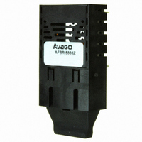
Manufacturer Part Number
AFBR-5803Z
Description
TXRX OPT 1X9 100MBPS DUPLEX SC
Manufacturer
Avago Technologies US Inc.
Datasheet
1.AFBR-5803ATZ.pdf
(16 pages)
Specifications of AFBR-5803Z
Data Rate
100Mbps
Wavelength
1300nm
Applications
General Purpose
Voltage - Supply
3.3V, 5V
Connector Type
SC
Mounting Type
Through Hole
Function
Implement FDDI and ATM at the 100 Mbps/125 MBd rate
Product
Transceiver
Pulse Width Distortion
0.69 ns (Max)/2.14 ns (Max)
Maximum Output Current
50 mA
Operating Supply Voltage
4.75 V to 5.25 V
Maximum Operating Temperature
+ 70 C
Minimum Operating Temperature
0 C
Lead Free Status / RoHS Status
Lead free / RoHS Compliant
For Use With
Multimode Glass
Lead Free Status / RoHS Status
Lead free / RoHS Compliant, Lead free / RoHS Compliant
Other names
516-1991


Solder and Wash Process Compatibility
The transceivers are delivered with protective process
plugs inserted into the duplex SC or duplex ST connector
receptacle. This process plug protects the optical subas-
semblies during wave solder and aqueous wash process-
ing and acts as a dust cover during shipping.
These transceivers are compatible with either industry
standard wave or hand solder processes.
Shipping Container
The transceiver is packaged in a shipping container
designed to protect it from mechanical and ESD damage
during shipment or storage.
Board Layout - Decoupling Circuit and Ground Planes
It is important to take care in the layout of your circuit
board to achieve optimum performance from these
transceivers. Figure 7 provides a good example of a
schematic for a power supply decoupling circuit that
works well with these parts. It is further recommended
that a contiguous ground plane be provided in the
circuit board directly under the transceiver to provide
a low inductance ground for signal return current. This
recommendation is in keeping with good high frequency
board layout practices.
Figure 8. Recommended Board Layout Hole Pattern
(0.800)
20.32
(0.100)
DIMENSIONS ARE IN MILLIMETERS (INCHES)
2.54
(0.800)
20.32
TOP VIEW
(0.075 ± 0.004)
2 x Ø 1.9 ± 0.1
(0.032 ± 0.004)
9 x Ø 0.8 ± 0.1
Board Layout - Hole Pattern
The Avago Technologies transceiver complies with the
circuit board “Common Transceiver Footprint” hole
pattern defined in the original multisource announce-
ment which defined the 1 x 9 package style. This drawing
is reproduced in Figure 8 with the addition of ANSI
Y14.5M compliant dimensioning to be used as a guide in
the mechanical layout of your circuit board.
Board Layout - Mechanical
For applications providing a choice of either a duplex SC
or a duplex ST connector interface, while utilizing the
same pinout on the printed circuit board, the ST port
needs to protrude from the chassis panel a minimum
of 9.53 mm for sufficient clearance to install the ST
connector.
Please refer to Figure 8a for a mechanical layout detailing
the recommended location of the duplex SC and duplex
ST transceiver packages in relation to the chassis panel.
Related parts for AFBR-5803Z
Image
Part Number
Description
Manufacturer
Datasheet
Request
R

Part Number:
Description:
650nm FE Transceiver Eval Kit
Manufacturer:
Avago Technologies US Inc.
Datasheet:

Part Number:
Description:
TXRX OPT OC3 MTRJ SFF 2X5DIP
Manufacturer:
Avago Technologies US Inc.
Datasheet:

Part Number:
Description:
TXRX ETHERNET 125MBD MMF 2X5
Manufacturer:
Avago Technologies US Inc.
Datasheet:

Part Number:
Description:
TXRX OPT SFP DGTL 850NM IND
Manufacturer:
Avago Technologies US Inc.
Datasheet:

Part Number:
Description:
TXRX OPT SFF 4/2/1GBD 2X7
Manufacturer:
Avago Technologies US Inc.
Datasheet:

Part Number:
Description:
TXRX OPT SFP 4/2/1GBD 850NM
Manufacturer:
Avago Technologies US Inc.
Datasheet:

Part Number:
Description:
TXRX OPT XFP 10GB/S 850NM
Manufacturer:
Avago Technologies US Inc.
Datasheet:

Part Number:
Description:
TXRX OPT 1X9 100MBPS ST EXT TEMP
Manufacturer:
Avago Technologies US Inc.
Datasheet:

Part Number:
Description:
TXRX OPT 1X9 100MBPS SC EXT TEMP
Manufacturer:
Avago Technologies US Inc.
Datasheet:

Part Number:
Description:
TXRX OPT 1X9 100MBPS DUPLEX ST
Manufacturer:
Avago Technologies US Inc.
Datasheet:

Part Number:
Description:
OPTOCOUPLER GATE DRV 2A 16-SOIC
Manufacturer:
Avago Technologies US Inc.
Datasheet:
Part Number:
Description:
OPTOCOUPLER 2CH 2.5A 16-SOIC
Manufacturer:
Avago Technologies US Inc.
Datasheet:

Part Number:
Description:
OPTOCOUPLER GATE DRV 0.4A 16SOIC
Manufacturer:
Avago Technologies US Inc.
Datasheet:

Part Number:
Description:
OPTOCOUPLER 2.0A 250KHZ 8-DIP
Manufacturer:
Avago Technologies US Inc.
Datasheet:

Part Number:
Description:
OPTOCOUPLER 2.0A 250KHZ GW 8-SMD
Manufacturer:
Avago Technologies US Inc.
Datasheet: