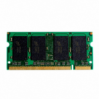
MT16LSDF6464HY-133D2 Micron Technology Inc, MT16LSDF6464HY-133D2 Datasheet - Page 8

MT16LSDF6464HY-133D2
Manufacturer Part Number
MT16LSDF6464HY-133D2
Description
MODULE SDRAM 512MB 144-SODIMM
Manufacturer
Micron Technology Inc
Datasheet
1.MT16LSDF6464HY-13ED2.pdf
(22 pages)
Specifications of MT16LSDF6464HY-133D2
Memory Type
SDRAM
Memory Size
512MB
Speed
133MHz
Package / Case
144-SODIMM
Main Category
DRAM Module
Sub-category
SDRAM
Module Type
144SODIMM
Device Core Size
64b
Organization
64Mx64
Total Density
512MByte
Chip Density
256Mb
Access Time (max)
6/5.4ns
Maximum Clock Rate
133MHz
Operating Supply Voltage (typ)
3.3V
Operating Current
1.096A
Number Of Elements
16
Operating Supply Voltage (max)
3.6V
Operating Supply Voltage (min)
3V
Operating Temp Range
0C to 65C
Operating Temperature Classification
Commercial
Pin Count
144
Mounting
Socket
Lead Free Status / RoHS Status
Lead free / RoHS Compliant
Available stocks
Company
Part Number
Manufacturer
Quantity
Price
Company:
Part Number:
MT16LSDF6464HY-133D2
Manufacturer:
MICRON
Quantity:
1 575
Company:
Part Number:
MT16LSDF6464HY-133D2 PCB
Manufacturer:
SIEMENS
Quantity:
201
M3 specifies the type of burst (sequential or inter-
leaved), M4–M6 specify the CL, M7 and M8 specify the
operating mode, M9 specifies the write burst mode,
and M10 and M11 are reserved for future use. For the
256MB and 512MB, M12 (A12) is undefined, but
should be driven LOW during loading of the mode reg-
ister.
banks are idle, and the controller must wait the speci-
fied time before initiating the subsequent operation.
Violating either of these requirements will result in
unspecified operation.
Burst Length
ented, with the burst length being programmable, as
shown in Figure 4. The burst length determines the
maximum number of column locations that can be
accessed for a given READ or WRITE command. Burst
lengths of 1, 2, 4, or 8 locations are available for both
the sequential and the interleaved burst types, and a
full-page burst is available for the sequential type. The
full-page burst is used in conjunction with the BURST
TERMINATE command to generate arbitrary burst
lengths.
operation or incompatibility with future versions may
result.
of columns equal to the burst length is effectively
selected. All accesses for that burst take place within
this block, meaning that the burst will wrap within the
block if a boundary is reached, as shown in Table 7 on
page 9. The block is uniquely selected by A1–A9 when
the burst length is set to two; by A2–A9 when the burst
length is set to four; and by A3–A9 when the burst
length is set to eight. The remaining (least significant)
address bit(s) is (are) used to select the starting loca-
tion within the block. Full-page bursts wrap within the
page if the boundary is reached, as shown in Table 7 on
page 9.
pdf: 09005aef807924d2, source: 09005aef807924f1
SDF16C32_64x64HG.fm - Rev. E 4/06 EN
Mode register bits M0–M2 specify the burst length,
The mode register must be loaded when all device
Read and write accesses to the SDRAM are burst ori-
Reserved states should not be used, as unknown
When a READ or WRITE command is issued, a block
8
256MB Module
512MB Module
compatibility with
to ensure compatibility
M11 and M10 = “0, 0”
*Should program
M12, M11, and
with future devices.
M10 = “0, 0, 0”
future devices.
*Should program
Figure 4: Mode Register Definition
to ensure
Micron Technology, Inc., reserves the right to change products or specifications without notice.
12
Reserved* WB
A12
Reserved* WB
11
11
A11
A11
10
10
A10
A10
144-PIN SDRAM SODIMM
256MB, 512MB (x64, DR)
M9
0
1
9
9
A9
A9
Op Mode
Op Mode
8
8
A8
A8
Programmed burst length
7
7
A7 A6 A5 A4 A3
A7 A6 A5 A4 A3
Single location access
M8
Diagram
CAS Latency BT
CAS Latency BT
0
-
Write Burst Mode
6
6
5
5
M7
0
-
4
4
©2006 Micron Technology, Inc. All rights reserved.
M3
Defined
M6-M0
0
1
3
3
M6
M2
-
0
0
0
0
1
1
1
1
0
0
0
0
1
1
1
1
Burst Length
Burst Length
M5
2
2
M1
A2 A1 A0
A2 A1 A0
0
0
1
1
0
0
1
1
0
0
1
1
0
0
1
1
M4
M0
Operating Mode
Standard operation
All other states reserved
1
1
0
1
0
1
0
1
0
1
0
1
0
1
0
1
0
1
0
0
Full Page
Reserved
Reserved
Reserved
Burst Type
Interleaved
M3 = 0
Sequential
1
2
4
8
Burst Length
Mode Register (Mx)
Mode Register (Mx)
CAS Latency
Address Bus
Address Bus
Reserved
Reserved
Reserved
Reserved
Reserved
Reserved
2
3
Reserved
Reserved
Reserved
Reserved
M3 = 1
1
2
4
8


