HYS72T128420HFA-3S-B Qimonda, HYS72T128420HFA-3S-B Datasheet - Page 4
HYS72T128420HFA-3S-B
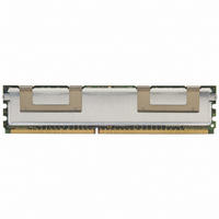
Manufacturer Part Number
HYS72T128420HFA-3S-B
Description
MODULE DDR2 1GB 240-DIMM
Manufacturer
Qimonda
Datasheet
1.HYS72T128420HFA-3S-B.pdf
(44 pages)
Specifications of HYS72T128420HFA-3S-B
Memory Type
DDR2 SDRAM
Memory Size
1GB
Speed
333MHz
Package / Case
240-DIMM
Lead Free Status / RoHS Status
Lead free / RoHS Compliant
Other names
675-1030


1.2
This document describes the electrical and mechanical
features of Qimonda’s 240-pin, PC2-4200F, PC2-5300F ECC
type, Fully Buffered Double-Data-Rate Two Synchronous
DRAM Dual In-Line Memory Modules (DDR2 SDRAM FB-
DIMMs). Fully Buffered DIMMs use commodity DRAMs
isolated from the memory channel behind a buffer on the
DIMM. They are intended for use as main memory when
installed in systems such as servers and workstations. PC2-
4200, PC2-5300 refers to the DIMM naming convention
indicating the DDR2 SDRAMs running at 266, 333 MHz clock
speed and offering 4200, 5300 MB/s peak bandwidth. FB-
DIMM features a novel architecture including the Advanced
Memory Buffer. This single chip component, located in the
center of each DIMM, acts as a repeater and buffer for all
signals and commands which are exchanged between the
host controller and the DDR2 SDRAMs including data in- and
output. The AMB communicates with the host controller and /
or the adjacent DIMMs on a system board using an Industry
1) All product types end with a place code, designating the silicon die revision. Example: HYS 72T64000HFA-3.7-A, indicating Rev. A dice
2) The Compliance Code is printed on the module label and describes the speed grade, e.g. “PC2-4200F-444-11-A”, where 4200F means
Rev. 1.00, 2006-10
10062006-RQWY-GI6S
Product Type
PC2-4200F (DDR2-533):
HYS72T64400HFA–3.7–B
HYS72T128420HFA–3.7–B
HYS72T256420HFA–3.7–B
PC2-5300F (DDR2-667):
HYS72T64400HFA–3S–B
HYS72T128420HFA–3S–B
HYS72T256420HFA–3S–B
DIMM
Density
512 MB
1 GB
2 GB
are used for DDR2 SDRAM components. To learn more on QIMONDA DDR2 module and component nomenclature see section 8 of this
datasheet.
Fully Buffered DIMM with 4.26 GB/sec. Module Bandwidth and “444-11” means CAS latency = 4, t
JEDEC SPD Revision 1.1 and assembled on Raw Card “A”.
Module
Organization
64M ×72
128M ×72
256M ×72
1)
Description
Compliance Code
512MB 1Rx8 PC2–4200F–444–11–A
1GB 2Rx8 PC2–4200F–444–11–B
2GB 2Rx4 PC2–4200F–444–11–H
512MB 1Rx8 PC2–4200F–444–11–A
1GB 2Rx8 PC2–4200F–444–11–B
2GB 2Rx4 PC2–4200F–444–11–H
Memory
Ranks
1
2
2
ECC/
Non-ECC
ECC
ECC
ECC
2)
Ordering Information (Pb-free components and assembly)
4
Standard
Interface at 1.5 V.
The Advanced Memory Buffer also allows buffering of
memory traffic to support large memory capacities. All
memory control for the DRAM resides in the host, including
memory request initiation, timing, refresh, scrubbing, sparing,
configuration
Advanced Memory Buffer interface is responsible for handling
channel and memory requests to and from the local DIMM
and for forwarding requests to other DIMMs on the memory
channel. Fully Buffered DIMM provides a high memory
bandwidth, large capacity channel solution that has a narrow
host interface. The maximum memory capacity is 288 DDR2
SDRAM devices per channel or 8 DIMMs.
# of
SDRAMs
9
18
36
HYS72T[64/128/256]4[00/20]HFA–[3S/3.7]–B
High-Speed
Description
1 Rank, FB-DIMM
2 Ranks, FB-DIMM
2 Ranks, FB-DIMM
1 Rank, FB-DIMM
2 Ranks, FB-DIMM
2 Ranks, FB-DIMM
# of row/bank/columns bits
13/2/10
13/2/10
13/2/11
access,
and
rcd
Differential
latency = 4 and t
power
SDRAM Technology
512 Mbit (x8)
512 Mbit (x8)
512 Mbit (x4)
512 Mbit (x8)
512 Mbit (x8)
512 Mbit (x4)
Internet Data Sheet
Point-to-Point
management.
Address Format
rp
latency = 4 using
TABLE 2
TABLE 3
Raw
Card
A
B
H
Link
The
Related parts for HYS72T128420HFA-3S-B
Image
Part Number
Description
Manufacturer
Datasheet
Request
R

Part Number:
Description:
BGA
Manufacturer:
Qimonda
Datasheet:
Part Number:
Description:
BGA
Manufacturer:
Qimonda
Datasheet:
Part Number:
Description:
Manufacturer:
Qimonda
Datasheet:
Part Number:
Description:
Manufacturer:
Qimonda
Datasheet:
Part Number:
Description:
DDR2 16Mx16, 667MHz, FBGA84, leadfree
Manufacturer:
Qimonda
Datasheet:
Part Number:
Description:
DDR2 32Mx16, 533MHz, FBGA84, leadfree
Manufacturer:
Qimonda
Datasheet:

Part Number:
Description:
HYB18TC1G160BF-3.71-Gbit DDR2 SDRAM
Manufacturer:
QIMONDA Qimonda AG
Datasheet:
Part Number:
Description:
HYB18TC1G800BF-3S1-Gbit DDR2 SDRAM
Manufacturer:
QIMONDA Qimonda AG
Datasheet: