HYS72T128420HFA-3S-B Qimonda, HYS72T128420HFA-3S-B Datasheet
HYS72T128420HFA-3S-B
Specifications of HYS72T128420HFA-3S-B


Related parts for HYS72T128420HFA-3S-B


HYS72T128420HFA-3S-B Summary of contents
Page 1
Cover Page – – ...
Page 2
... Any information within this document that you feel is wrong, unclear or missing at all? Your feedback will help us to continuously improve the quality of this document. Please send your proposal (including a reference to this document) to: techdoc@qimonda.com qag_techdoc_rev400 / 3.2 QAG / 2006-07-21 10062006-RQWY-GI6S HYS72T[64/128/256]4[00/20]HFA–[3S/3.7]–B ...
Page 3
... Overview This chapter describes the main characteristics of the 240-Pin Fully-Buffered DDR2 SDRAM Modules product family. 1.1 Features • 240-pin Fully-Buffered ECC Dual-In-Line DDR2 SDRAM Module for PC, Workstation and Server main memory applications. • Module organisation one rank 64M x 72, one rank 128M x 72, two ranks 128M x 72, two ranks 256M x 72 • ...
Page 4
... PC2–4200F–444–11–H PC2-5300F (DDR2-667): HYS72T64400HFA–3S–B 512MB 1Rx8 PC2–4200F–444–11–A HYS72T128420HFA–3S–B 1GB 2Rx8 PC2–4200F–444–11–B HYS72T256420HFA–3S–B 2GB 2Rx4 PC2–4200F–444–11–H 1) All product types end with a place code, designating the silicon die revision. Example: HYS 72T64000HFA-3.7-A, indicating Rev. A dice are used for DDR2 SDRAM components ...
Page 5
... Product Type DRAM components HYS72T64000HF HYB18T512800BF HYS72T128020HF HYB18T512800BF HYS72T256020HF HYB18T512400BF 1) Green Product 1) For a detailed description of all functionalities of the DRAM components on these modules see the component datasheet. Rev. 1.00, 2006-10 10062006-RQWY-GI6S HYS72T[64/128/256]4[00/20]HFA–[3S/3.7]–B Components on Modules 1) DRAM Density DRAM Organisation 64M ×8 512 Mbit 64M × ...
Page 6
Pin Configuration The pin configuration of the DDR2 SDRAM DIMM is listed by function in Pin and Buffer Type are explained in Table 6 Pin# Clock Signals 228 229 Control Signals 17 Northbound ...
Page 7
Pin 142 145 148 151 154 157 171 174 177 180 183 186 168 160 143 146 149 152 155 158 172 175 178 181 184 187 169 161 Southbound ...
Page 8
Pin# 102 100 103 91 190 193 196 199 202 213 216 219 222 210 191 194 197 200 203 214 217 220 223 211 EEPROM 120 119 239 240 118 Power ...
Page 9
Pin# 9,10,12,13,129,130,132,133 15,117,135,237 1,2,3,5,6,7,108,109,111,112,113,115 ,116,121,122,123,125,126, 127,231,232,233,235,236 4,8,11,14,18,21,24,27,30,33,36, 39,42,43,46,47,50,53,56,59,62, 65,68,69,72,75,78,81,84,85,88, 89,92,95,98,101,104,107,110, 114,124,128,131,134,138,141, 144,147,150,153,156,159,162, 163,166,167,170,173,176,179, 182,185,188,189,192,195,198, 201,204,205,208,209,212,215, 218,221,224,227,230,234 Other Pins 19,20,44,45,86,87,105,106,139, 140,164,165,206,207,225,226 136 16 137 Abbreviation HSDL_15 LV-CMOS CMOS OD Rev. 1.00, 2006-10 10062006-RQWY-GI6S HYS72T[64/128/256]4[00/20]HFA–[3S/3.7]–B Name Pin Buffer Type Type V PWR ...
Page 10
Abbreviation I O I/O AI PWR GND NU NC Rev. 1.00, 2006-10 10062006-RQWY-GI6S HYS72T[64/128/256]4[00/20]HFA–[3S/3.7]–B Description Standard input-only pin. Digital levels. Output. Digital levels. I bidirectional input/output signal. Input. Analog levels. Power Ground Not Usable Not Connected 10 Internet ...
Page 11
Rev. 1.00, 2006-10 10062006-RQWY-GI6S HYS72T[64/128/256]4[00/20]HFA–[3S/3.7]–B Pin Configuration for FB-DIMM (240 pin) 11 Internet Data Sheet FIGURE 1 ...
Page 12
Input/Output Functional Description Symbol Type Polarity Channel Signals SCK, SCK Input Differential PN[13:0], PN[13:0] Output Differential PS[9:0], PS[9:0] Input Differential SN[13:0], SN[13:0] Input Differential SS[9:0], SS[9:0] Output Differential SMB Bus Signals SA[2:0] Input — SDA I/O — SCL Input ...
Page 13
Basic Functionality The Advanced Memory Buffer (AMB) reference design complies with the FB-DIMM Architecture and Protocol Specification. 4.1 Advanced Memory Buffer Functionality The Advanced Memory Buffer will perform the following FB- DIMM channel functions: • Supports channel initialization procedures ...
Page 14
Interface Topology The FB-DIMM channel uses a daisy-chain topology to provide expansion from a single DIMM per channel DIMMs per channel. The host sends data on the southbound link to the first DIMM where it is ...
Page 15
High-Speed Differential Point-to-Point Link (at 1.5 V) Interfaces The Advanced Memory Buffer supports one FB-DIMM Channel consisting of two bidirectional link interfaces using highspeed differential point-to-point electrical signaling. The southbound input link is 10 lanes wide and carries commands ...
Page 16
Peak Theoretical Channel Throughput An FB-DIMM channel transfers read completion data on the Northbound data connection. 144 bits of data are transferred for every Northbound data frame. This matches the 18-byte data transfer of an ECC DDR DRAM in ...
Page 17
Electrical Characteristics 5.1 Operating Conditions Symbol Parameter V V Voltage on pin relative Voltage on pin relative Voltage on pin relative to DDQ DDQ V V Voltage on pin ...
Page 18
Parameter Symbol AMB Supply Voltage V CC DRAM Supply Voltage V DD Termination Voltage V TT EEPROM Supply Voltage V DDSPD DC Input Logic High(SPD) V IH(DC) DC Input Logic Low(SPD) V IL(DC) DC Input Logic High(RESET) V IH(DC) DC ...
Page 19
Parameter Operating Temperature Operating Humidity (relative) Storage Temperature Storage Humidity (without condensation) Barometric pressure (operating) Barometric pressure (storage) 1) The designer must meet the case temperature specifications for individual module components. 2) Stresses greater than those listed may cause permanent ...
Page 20
Current Spec. and Conditions The following table provides an overview of the measurement conditions. Parameter Idle Current, single or last DIMM L0 state, idle (0 BW) Primary channel enabled, Secondary channel disabled CKE high. Command and address lines stable. ...
Page 21
Parameter MemBIST Over all MemBIST modes >50% DRAM BW (as dictated by the AMB) Primary channel Enabled Secondary channel Enabled CKE high. Command and Address lines stable DRAM clock active Electrical Idle DRAM Idle (0 BW) Primary channel Disabled Secondary ...
Page 22
... Measured currents on raw card A/B/H/D according to the INTEL/ JEDEC specifcation.The measurements are done in a INTEL Blackford system The Power is calculated as follows Rev. 1.00, 2006-10 10062006-RQWY-GI6S HYS72T[64/128/256]4[00/20]HFA–[3S/3.7]–B HYS72T128420HFA-3S-B PC2-5300F Max. 1.67 2.54 1.16 2.05 2.88 4.64 2.69 4.03 1 ...
Page 23
... PTOT_EI 3.32 ICC_MEMBIST 2.82 PCC_MEMBIST 4.22 IDD_MEMBIST 2.13 PDD_MEMBIST 3.76 ITOT_MEMBIST 4.96 PTOT_MEMBIST 7.99 Rev. 1.00, 2006-10 10062006-RQWY-GI6S HYS72T[64/128/256]4[00/20]HFA–[3S/3.7]–B HYS72T128420HFA-3S-B HYS72T256420HFA-3S-B PC2-5300F PC2-5300F Max. Max. 6.56 7.92 3.02 3.01 4.51 4.5 0.96 1.72 1.7 3.04 4.02 4.8 6 ...
Page 24
... PTOT_IBIST 5.39 ICC_Training 2.68 PCC_Training 4.03 IDD_Trainig 0.6 PDD_Training 1.06 ITOT_Trainig 3.33 Rev. 1.00, 2006-10 10062006-RQWY-GI6S HYS72T[64/128/256]4[00/20]HFA–[3S/3.7]– HYS72T128420HFA-3.7-B HYS72T256420HFA-3.7-B PC2-4200F PC2-4200F Max. Max. 1.5 1.52 2.29 2.28 1.09 1.92 1.93 3.34 2.65 3.52 4.27 5.71 2.43 2.45 3 ...
Page 25
... PTOT_EI 2.99 ICC_MEMBIST 2.54 PCC_MEMBIST 3.82 IDD_MEMBIST 2.06 PDD_MEMBIST 3.64 ITOT_MEMBIST 4.66 PTOT_MEMBIST 7.51 Rev. 1.00, 2006-10 10062006-RQWY-GI6S HYS72T[64/128/256]4[00/20]HFA–[3S/3.7]–B HYS72T128420HFA-3.7-B HYS72T256420HFA-3.7-B PC2-4200F PC2-4200F Max. Max. 5.65 6.86 1.86 1.89 2.82 2.82 0.11 0.26 0.2 0.36 2.04 2.25 3 ...
Page 26
SPD Codes This chapter lists all hexadecimal byte values stored in the EEPROM of the products described in this data sheet. SPD stands for serial presence detect. All values with XX in the table are module specific bytes which ...
Page 27
Product Type Organization Label Code JEDEC SPD Revision Byte# Description t 14 (min. CAS Latency Time) CAS.MIN 15 Write Recovery Values Supported (WR (Write Recovery Time) WR.MIN 17 Write Latency Times Supported 18 Additive Latency Times Supported t ...
Page 28
Product Type Organization Label Code JEDEC SPD Revision Byte# Description ∆ (DT5B) DRAM 5B ∆ (DT7) DRAM Not used 79 FBDIMM ODT Values 80 Not used 81 Channel Protocols Supported LSB 82 ...
Page 29
Product Type Organization Label Code JEDEC SPD Revision Byte# Description 105 AMB Personality Bytes: Pre-initialization (5) 106 AMB Personality Bytes: Pre-initialization (6) 107 AMB Personality Bytes: Post-initialization (1) 108 AMB Personality Bytes: Post-initialization (2) 109 AMB Personality Bytes: Post-initialization (3) ...
Page 30
Product Type Organization Label Code JEDEC SPD Revision Byte# Description 133 Module Product Type, Char #6 134 Module Product Type, Char #7 135 Module Product Type, Char #8 136 Module Product Type, Char #9 137 Module Product Type, Char #10 ...
Page 31
Product Type Organization Label Code JEDEC SPD Revision Byte# Description 0 SPD Size CRC / Total / Used 1 SPD Revision 2 Key Byte / DRAM Device Type 3 Voltage Level of this Assembly 4 SDRAM Addressing 5 Module Physical ...
Page 32
Product Type Organization Label Code JEDEC SPD Revision Byte# Description t 23 (min. Active to Precharge Time) RAS.MIN t 24 (min. Active to Active / Refresh Time) RC.MIN t 25 LSB (min. Refresh Recovery Time Delay) RFC.MIN t 26 MSB ...
Page 33
Product Type Organization Label Code JEDEC SPD Revision Byte# Description 85 AMB Read Access Delay for DDR2-667 86 AMB Read Access Delay for DDR2-533 87 Psi(T-A) AMB ∆ (DT Idle_0) AMB Idle_0 ∆ (DT Idle_1) AMB ...
Page 34
Product Type Organization Label Code JEDEC SPD Revision Byte# Description 114 AMB Personality Bytes: Post-initialization (8) 115 AMB Manufacturers JEDEC ID Code LSB 116 AMB Manufacturers JEDEC ID Code MSB 117 DIMM Manufacturers JEDEC ID Code LSB 118 DIMM Manufacturers ...
Page 35
Product Type Organization Label Code JEDEC SPD Revision Byte# Description 142 Module Product Type, Char #15 143 Module Product Type, Char #16 144 Module Product Type, Char #17 145 Module Product Type, Char #18 146 Module Revision Code 147 Test ...
Page 36
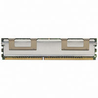
... L-DIM-240-22 R/C H L-DIM-240-25 1) Thickness includes Qimonda Heat Sink. Some early production modules with Jedec Heatspreader may be thicker up to 8.2mm. Attention: Heat Sink heat up during operation. When unplugging a DIMM from a system direct skin contact should be avoided until the Heat Sink has reached room temperature. ...
Page 37
Notes 1. Please contact your sales or marketing representative for more details on package dimensions. Rev. 1.00, 2006-10 10062006-RQWY-GI6S HYS72T[64/128/256]4[00/20]HFA–[3S/3.7]–B Package Outline L-DIM-240-21 with Full Heat Sink 2. Drawing according to ISO 8015 3. Dimensions General tolerances ...
Page 38
Notes 1. Please contact your sales or marketing representative for more details on package dimensions. Rev. 1.00, 2006-10 10062006-RQWY-GI6S HYS72T[64/128/256]4[00/20]HFA–[3S/3.7]–B Package Outline L-DIM-240-22 with Full Heat Sink 2. Drawing according to ISO 8015 3. Dimensions General tolerances ...
Page 39
Notes 1. Please contact your sales or marketing representative for more details on package dimensions. Rev. 1.00, 2006-10 10062006-RQWY-GI6S HYS72T[64/128/256]4[00/20]HFA–[3S/3.7]–B Package Outline L-DIM-240-25 with Full Heat Sink 2. Drawing according to ISO 8015 3. Dimensions General tolerances ...
Page 40
DDR2 Nomencature Example for Field Number 1 2 Micro-DIMM HYS 64 DDR2 DRAM HYB 18 Rev. 1.00, 2006-10 10062006-RQWY-GI6S HYS72T[64/128/256]4[00/20]HFA–[3S/3.7]– 64128 5121G Internet Data Sheet TABLE ...
Page 41
... Field Description 1 QIMONDA Module Prefix 2 Module Data Width [bit] 3 DRAM Technology 4 Memory Density per I/O [Mbit]; 1) Module Density 5 Raw Card Generation 6 Number of Module Ranks 7 Product Variations 8 Package, Lead-Free Status 9 Module Type 10 Speed Grade 11 Die Revision 1) Multiplying “Memory Density per I/O” with “Module Data Width” and dividing by 8 for Non-ECC and 9 for ECC modules gives the overall module memory density in MBytes as listed in column “ ...
Page 42
... Field Description 1 QIMONDA Component Prefix 2 Interface Voltage [V] 3 DRAM Technology 4 Component Density [Mbit] 5+6 Number of I/Os 7 Product Variations 8 Die Revision 9 Package, Lead-Free Status 10 Speed Grade Rev. 1.00, 2006-10 10062006-RQWY-GI6S HYS72T[64/128/256]4[00/20]HFA–[3S/3.7]–B DDR2 DRAM Nomenclature Values Coding HYB Constant 18 SSTL_18 ...
Page 43
Table of Contents 1 Overview . . . . . . . . . . . . . . . . . . . . . . . . . . . . . . . . . . . ...
Page 44
... Due to technical requirements components may contain dangerous substances. For information on the types in question please contact your nearest Qimonda Office. Qimonda Components may only be used in life-support devices or systems with the express written approval of Qimonda failure of such components can reasonably be expected to cause the failure of that life-support device or system affect the safety or effectiveness of that device or system ...