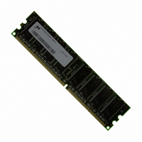
MT8VDDT6464AY-40BF4 Micron Technology Inc, MT8VDDT6464AY-40BF4 Datasheet - Page 16

MT8VDDT6464AY-40BF4
Manufacturer Part Number
MT8VDDT6464AY-40BF4
Description
MODULE DDR SDRAM 512MB 184-DIMM
Manufacturer
Micron Technology Inc
Datasheet
1.MT8VDDT6464AY-40BF4.pdf
(26 pages)
Specifications of MT8VDDT6464AY-40BF4
Memory Type
DDR SDRAM
Memory Size
512MB
Speed
400MT/s
Package / Case
184-DIMM
Lead Free Status / RoHS Status
Lead free / RoHS Compliant
Other names
557-1232
MT8VDDT6464AY-40BF4
MT8VDDT6464AY-40BF4
Notes
PDF: 09005aef80a43556, Source: 09005aef80a43534
DDA8C16_32_64x64AG_2.fm - Rev. E 4/06 EN
10. I
11. This parameter is sampled. V
12. For slew rates <1 V/ns and greater ≥0.5 V/ns. If slew rate is <0.5 V/ns, timing must be
13. Inputs are not recognized as valid until V
14. MIN (
15. The refresh period is 64ms. This equates to an average refresh rate of 15.625µs
1. All voltages referenced to V
2. Tests for AC timing, I
3. Outputs measured with equivalent load:
4. AC timing and I
5. The AC and DC input level specifications are as defined in the SSTL_2 Standard (i.e.,
6. V
7. V
8. I
9. Enables on-chip refresh and address counters.
at nominal reference/supply voltage levels, but the related specifications and device
operation are guaranteed for the full voltage range specified.
Output
(V
ment, but input timing is still referenced to V
and parameter specifications are guaranteed for the specified AC input levels under
normal use conditions. The minimum slew rate for the input signals used to test the
device is 1V/ns in the range between V
the receiver will effectively switch as a result of the signal crossing the AC input level,
and will remain in that state as long as the signal does not ring back above [below] the
DC input LOW [HIGH] level).
the DC level of the same. Peak-to-peak noise (non-common mode) on V
exceed ±2 percent of the DC value. From V
and an additional ±25mV for AC noise, measured at the nearest V
resistors, is expected to be set equal to V
of V
with minimum cycle time at CL = 3 for -40B with the outputs open.
the defined cycle rate.
MHz, T
with I/O pins, reflecting the fact that they are matched in loading.
derated:
500mV/ns, while
tain. For -40B, slew rates must be ≥0.5 V/ns.
before V
minimum absolute value for the respective parameter.
ments is the largest multiple of
(128MB), or 7.8125µs (256MB, 512MB). However, an AUTO REFRESH command must
be asserted at least once every 140.6µs (128MB) or 70.3µs (256MB, 512MB); burst
refreshing or posting by the DRAM controller greater than eight refresh cycles is not
allowed.
DD
DD
REF
TT
OUT
REF
is dependent on output loading and cycle rates. Specified values are obtained
specifications are tested after the device is properly initialized, and is averaged at
is not applied directly to the device. V
)
is expected to equal V
128MB, 256MB, 512MB (x64, SR): PC3200 184-Pin DDR UDIMM
t
RC or
.
A
REF
V
t
= 25°C, V
IS has an additional 50ps per each 100mV/ns reduction in slew rate from
TT
50
30pF
Reference
Point
stabilizes, CKE ≤ 0.3 × V
t
Ω
RFC) for I
DD
t
OUT
IH is unaffected. If slew rate exceeds 4.5 V/ns, functionality is uncer-
tests may use a V
DD
(
DC
DD
, and electrical AC and DC characteristics may be conducted
) = V
measurements is the smallest multiple of
DD
16
SS
.
DD
DD
Q/2 of the transmitting device and to track variations in
t
Q/2, V
CK that meets the maximum absolute value for
= +2.6V ±0.1V, V
DD
IL
Micron Technology, Inc., reserves the right to change products or specifications without notice.
-to-V
OUT
Q is recognized as LOW.
IL
REF
(
REF
AC
TT
DD
(peak to peak) = 0.2V. DM input is grouped
IH
, and must track variations in the DC level
) and V
REF
is a system supply for signal termination
stabilizes. Exception: during the period
Q/2, V
swing of up to 1.5V in the test environ-
(or to the crossing point for CK/CK#),
DD
IH
Q = +2.6V ±0.1V, V
REF
(
AC
is allowed ±25mV for DC error
t
).
RAS (MAX) for I
©2005 Micron Technology, Inc. All rights reserved.
REF
t
CK that meets the
bypass capacitor.
REF
DD
REF
= Vss, f = 100
measure-
may not
Notes
t
RAS.


