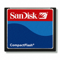
SDCFJ-1024-388 SanDisk, SDCFJ-1024-388 Datasheet - Page 51

SDCFJ-1024-388
Manufacturer Part Number
SDCFJ-1024-388
Description
COMPACT FLASH 1GB
Manufacturer
SanDisk
Type
CompactFlashr
Specifications of SDCFJ-1024-388
Memory Size
1GB
Memory Type
CompactFLASH
Density
1GByte
Operating Supply Voltage (typ)
3.3/5V
Operating Temperature (min)
0C
Operating Temperature (max)
70C
Package Type
Not Required
Mounting
Socket
Pin Count
50
Operating Temperature Classification
Commercial
Operating Supply Voltage (min)
3.135/4.5V
Operating Supply Voltage (max)
3.465/5.5V
Programmable
Yes
Lead Free Status / RoHS Status
Lead free / RoHS Compliant
ATA Drive Register Set Definition and Protocol
4.5.6. Cylinder Low (LBA 15-8) Register (Address—1F4[174]; Offset 4)
This register contains the low order 8 bits of the starting cylinder address or bits 15-8 of the Logical Block Address.
4.5.7. Cylinder High (LBA 23-16) Register (Address—1F5[175]; Offset 5)
This register contains the high order bits of the starting cylinder address or bits 23-16 of the Logical Block Address.
4.5.8. Drive/Head (LBA 27-24) Register (Address 1F6[176]; Offset 6)
The Drive/Head register is used to select the drive and head. It is also used to select LBA addressing instead of
cylinder/head/sector addressing. The bits are defined as follows:
Bit 7
Bit 6
Bit 5
Bit 4 (DRV)
Bit 3 (HS3)
Bit 2 (HS2)
Bit 1 (HS1)
Bit 0 (HS0)
4.5.9. Status & Alternate Status Registers (Address 1F7[177]&3F6[376]; Offsets 7 & Eh)
These registers return the CompactFlash Memory Card status when read by the host. Reading the Status register
does clear a pending interrupt while reading the Auxiliary Status register does not. The meaning of the status bits are
described as follows:
4-6
BUSY
D7
D7
1
This bit is set to 1.
LBA is a flag to select either Cylinder/Head/Sector (CHS) or Logical Block Address Mode (LBA). When
LBA=0, Cylinder/Head/Sector mode is selected. When LBA=1, Logical Block Address is selected. In
Logical Block Mode, the Logical Block Address is interpreted as follows:
LBA07-LBA00: Sector Number Register D7-D0.
LBA15-LBA08: Cylinder Low Register D7-D0.
LBA23-LBA16: Cylinder High Register D7-D0.
LBA27-LBA24: Drive/Head Register bits HS3-HS0.
This bit is set to 1.
This bit will have the following meaning. DRV is the drive number. When DRV=0, drive (card) 0 is selected
When DRV=1, drive (card) 1 is selected. The CompactFlash Card is set to be Card 0 or 1 using the copy field
of the PCMCIA Socket & Copy configuration register.
When operating in the Cylinder , Head, Sector mode, this is bit 3 of the head number. It is Bit 27 in the
Logical Block Address mode.
When operating in the Cylinder, Head, Sector mode, this is bit 2 of the head number. It is Bit 26 in the
Logical Block Address mode.
When operating in the Cylinder, Head, Sector mode, this is bit 1 of the head number. It is Bit 25 in the
Logical Block Address mode.
When operating in the Cylinder, Head, Sector mode, this is bit 0 of the head number. It is Bit 24 in the
Logical Block Address mode.
RDY
LBA
D6
D6
DWF
D5
D5
1
CompactFlash
DRV
DSC
D4
D4
®
Memory Card Product Manual, Rev. 11.0 ©2006 SanDisk Corporation
DRQ
HS3
D3
D3
CORR
HS2
D2
D2
HS1
D1
D1
0
ERR
HS0
D0
D0


