DS1904L-F5# Maxim Integrated Products, DS1904L-F5# Datasheet - Page 9
DS1904L-F5#
Manufacturer Part Number
DS1904L-F5#
Description
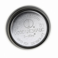
IBUTTON RTC F5 MICROCAN
Manufacturer
Maxim Integrated Products
Series
iButton®r
Datasheet
1.DS1904L-F5.pdf
(13 pages)
Specifications of DS1904L-F5#
Rohs Information
IButton RoHS Compliance Plan
Lead Free Status / RoHS Status
Lead free / RoHS Compliant
Memory Size
-
Memory Type
-
Lead Free Status / Rohs Status
Lead free / RoHS Compliant
Available stocks
Company
Part Number
Manufacturer
Quantity
Price


Skip ROM [CCh]
This command can save time in a single drop bus system by allowing the bus master to access the clock
functions without providing the 64-bit ROM code. If more than one slave is present on the bus and, for
example, a read command is issued following the Skip ROM command, data collision will occur on the
bus as multiple slaves transmit simultaneously (open drain pull-downs will produce a wired-AND result).
1–WIRE SIGNALING
The DS1904 requires strict protocols to ensure data integrity. The protocol consists of four types of sig-
naling on one line: Reset Sequence with Reset Pulse and Presence Pulse, Write 0, Write 1 and Read Data.
Except for the presence pulse the bus master initiates all these signals.
The initialization sequence required to begin any communication with the DS1904 is shown in Figure 8.
A reset pulse followed by a presence pulse indicates the DS1904 is ready to send or receive data. The bus
master transmits (TX) a reset pulse (t
goes into receive mode (RX). The 1-Wire bus is pulled to a high state via the pull-up resistor. After
detecting the rising edge on the data line, the DS1904 waits (t
presence pulse (t
INITIALIZATION PROCEDURE “RESET AND PRESENCE PULSES” Figure 8
READ/WRITE TIME SLOTS
The definitions of write and read time slots are illustrated in Figure 9. The master initiates all time slots
by driving the data line low. The falling edge of the data line synchronizes the DS1904 to the master by
triggering an internal delay circuit. During write time slots, the delay circuit determines when the DS1904
will sample the data line. For a read data time slot, if a “0” is to be transmitted, the delay circuit deter-
mines how long the DS1904 will hold the data line low. If the data bit is a “1”, the DS1904 will not hold
the data line low at all.
*
**
V
PULLUP MIN
V
V
PULLUP
V
In order not to mask interrupt signaling by other devices on the 1-Wire bus t
ways be less than 960 µs.
Includes recovery time
IL MAX
IH MIN
0V
PDL
RESISTOR
MASTER
DS1904
, 60-240 s).
"RESET PULSE"
MASTER TX
t
RSTL
RSTL
480 µs t
480 µs t
15 µs t
60 t
, minimum 480 s). The bus master then releases the line and
PDL
t
R
PDH
< 240 µs
RSTL
RSTH
MASTER RX "PRESENCE PULSE"
9 of 13
t
< 60 µs
PDH
<
<
*
**
t
PDH
PDL
t
RSTH
, 15-60 s) and then transmits the
RSTL
+ t
R
should al-
Related parts for DS1904L-F5#
Image
Part Number
Description
Manufacturer
Datasheet
Request
R

Part Number:
Description:
RTC Ibutton
Manufacturer:
Maxim Integrated Products
Datasheet:
Part Number:
Description:
MAX7528KCWPMaxim Integrated Products [CMOS Dual 8-Bit Buffered Multiplying DACs]
Manufacturer:
Maxim Integrated Products
Datasheet:
Part Number:
Description:
Single +5V, fully integrated, 1.25Gbps laser diode driver.
Manufacturer:
Maxim Integrated Products
Datasheet:
Part Number:
Description:
Single +5V, fully integrated, 155Mbps laser diode driver.
Manufacturer:
Maxim Integrated Products
Datasheet:
Part Number:
Description:
VRD11/VRD10, K8 Rev F 2/3/4-Phase PWM Controllers with Integrated Dual MOSFET Drivers
Manufacturer:
Maxim Integrated Products
Datasheet:
Part Number:
Description:
Highly Integrated Level 2 SMBus Battery Chargers
Manufacturer:
Maxim Integrated Products
Datasheet:
Part Number:
Description:
Current Monitor and Accumulator with Integrated Sense Resistor; ; Temperature Range: -40°C to +85°C
Manufacturer:
Maxim Integrated Products
Part Number:
Description:
TSSOP 14/A�/RS-485 Transceivers with Integrated 100O/120O Termination Resis
Manufacturer:
Maxim Integrated Products
Part Number:
Description:
TSSOP 14/A�/RS-485 Transceivers with Integrated 100O/120O Termination Resis
Manufacturer:
Maxim Integrated Products
Part Number:
Description:
QFN 16/A�/AC-DC and DC-DC Peak-Current-Mode Converters with Integrated Step
Manufacturer:
Maxim Integrated Products
Part Number:
Description:
TDFN/A/65V, 1A, 600KHZ, SYNCHRONOUS STEP-DOWN REGULATOR WITH INTEGRATED SWI
Manufacturer:
Maxim Integrated Products
Part Number:
Description:
Integrated Temperature Controller f
Manufacturer:
Maxim Integrated Products
Part Number:
Description:
SOT23-6/I�/45MHz to 650MHz, Integrated IF VCOs with Differential Output
Manufacturer:
Maxim Integrated Products
Part Number:
Description:
SOT23-6/I�/45MHz to 650MHz, Integrated IF VCOs with Differential Output
Manufacturer:
Maxim Integrated Products
Part Number:
Description:
EVALUATION KIT/2.4GHZ TO 2.5GHZ 802.11G/B RF TRANSCEIVER WITH INTEGRATED PA
Manufacturer:
Maxim Integrated Products