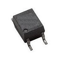
HCPL-M454#500 Avago Technologies US Inc., HCPL-M454#500 Datasheet - Page 7

HCPL-M454#500
Manufacturer Part Number
HCPL-M454#500
Description
OPTOCOUPLER 1MBS TTL/IPM SO-5
Manufacturer
Avago Technologies US Inc.
Datasheet
1.HCPL-M454500.pdf
(12 pages)
Specifications of HCPL-M454#500
Input Type
DC
Package / Case
5-SOP
Number Of Channels
1
Voltage - Isolation
3750Vrms
Current Transfer Ratio (min)
25% @ 16mA
Current Transfer Ratio (max)
60% @ 16mA
Voltage - Output
20V
Current - Output / Channel
8mA
Current - Dc Forward (if)
25mA
Output Type
Transistor with Vcc
Mounting Type
Surface Mount
Isolation Voltage
3750 Vrms
Output Device
Phototransistor
Configuration
1 Channel
Current Transfer Ratio
65 %
Maximum Baud Rate
1 MBps
Maximum Forward Diode Voltage
1.7 V
Maximum Reverse Diode Voltage
5 V
Maximum Input Diode Current
25 mA
Maximum Power Dissipation
100 mW
Maximum Operating Temperature
+ 70 C
Minimum Operating Temperature
0 C
Lead Free Status / RoHS Status
Contains lead / RoHS non-compliant
Vce Saturation (max)
-
Lead Free Status / RoHS Status
Lead free / RoHS Compliant, Contains lead / RoHS non-compliant
Available stocks
Company
Part Number
Manufacturer
Quantity
Price
Notes:
10. The R
11. Use of a 0.1 µF bypass capacitor connected between pins 4 and 6 is recommended.
12. In accordance with UL 1577, each optocoupler is proof tested by applying an insulation test voltage ≥4500 V
13. The difference between t
Figure 1. DC and Pulsed Transfer Characteristics.
Figure 4. Current Transfer Ratio vs. Temperature.
1. Derate linearly above 70°C free-air temperature at a rate of 0.8 mA/°C.
2. Derate linearly above 70°C free-air temperature at a rate of 1.6mA/°C.
3. Derate linearly above 70°C free-air temperature at a rate of 0.9 mA/°C.
4. Derate linearly above 70°C free-air temperature at a rate of 2.0 mA/°C.
5. CURRENT TRANSFER RATIO in percent is defined as the ratio of output collector current (I
6. Device considered a two-terminal device: Pins 1 and 3 shorted together and Pins 4, 5 and 6 shorted together.
7. Under TTL load and drive conditions: Common mode transient immunity in a Logic High level is the maximum tolerable (positive) dV
8. Under IPM (Intelligent Power Module) load and LED drive conditions: Common mode transient immunity in a Logic High level is the maxi-
9. The 1.9 kΩ load represents 1 TTL unit load of 1.6 mA and the 5.6 kΩ pull-up resistor.
10
the leading edge of the common mode pulse, V
transient immunity in a Logic Low level is the maximum tolerable (negative) dV
V
mum tolerable dV
V
mode pulse signal,V
tion current limit, I
Propagation Delay Specifications section).
1.1
1.0
0.9
0.8
0.7
0.6
5
0
O
CM
-60
0
> 3.0 V). Common mode transient immunity in a Logic Low level is the maximum tolerable dV
T = 25°C
V
, to assure that the output will remain in a Logic Low state (i.e., V
A
CC
L
-40 -20 0
= 20 kΩ, C
V
= 5.0 V
O
NORMALIZED
I
V
V
T
F
T
O
CC
A
– OUTPUT VOLTAGE – V
A
= 16 mA
= 0.4 V
= 25°C
HCPL-M454 fig 1
– TEMPERATURE – °C
= 5.0 V
HCPL-M454 fig 4
L
CM
= 100 pF load represents an IPM (Intelligent Power Mode) load.
i-e
20 40 60 80 100 120
10
CM
/dt on the leading edge of the common mode pulse, V
≤ 5 µA).
, to assure that the output will remain in a Logic Low state (i.e., V
PLH
and t
I = 5 mA
40 mA
35 mA
30 mA
25 mA
20 mA
15 mA
10 mA
F
PHL
, between any two HCPL-M454 parts under the same test condition. (See Power Inverter Dead Time and
20
Figure 2. Current Transfer Ratio vs. Input Current.
Figure 5. Logic High Output Current vs. Temperature.
CM
1.5
1.0
0.5
0.0
10
10
, to assure that the output will remain in a Logic High state (i.e., V
10
10
10
10
10
-2
-1
4
3
2
1
0
-60
0
2 4 6 8 10 12 14 16 18
-40 -20
I
F
I
V
F
T
– INPUT CURRENT – mA
O
A
= 0 mA
= V
HCPL-M454 fig 2
– TEMPERATURE – °C
HCPL-M454 fig 5
0
CC
O
= 5.0 V
20 40 60 80 100 120
< 0.8 V).
CM
NORMALIZED
I
V
V
T
F
CC
A
O
, to assure that the output will remain in a Logic High state (i.e.,
= 16 mA
= 25°C
= 0.4 V
CM
20 22 24 26
= 5.0 V
/dt on the trailing edge of the common mode pulse signal,
O
< 1.0 V).
O
), to the forward LED input current (I
CM
Figure 3. Input Current vs. Forward Voltage.
/dt on the trailing edge of the common
0.001
1000
0.01
100
1.0
0.1
10
1.1
V
F
– FORWARD VOLTAGE – VOLTS
RMS
1.2
V
for 1 second (leakage detec-
+
–
F
I
F
O
> 2.0 V). Common mode
HCPL-M454 fig 3
1.3
1.4
F
T = 25°C
), times 100.
A
1.5
CM
/dt on
1.6


