H11D2 Vishay, H11D2 Datasheet - Page 3
H11D2
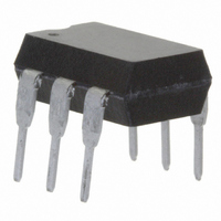
Manufacturer Part Number
H11D2
Description
OPTOCOUPLER PHOTOTRANS 20% 6DIP
Manufacturer
Vishay
Datasheet
1.H11D3.pdf
(8 pages)
Specifications of H11D2
Isolation Voltage
5300 Vrms
Number Of Channels
1
Input Type
DC
Voltage - Isolation
5300Vrms
Current Transfer Ratio (min)
20% @ 10mA
Voltage - Output
300V
Current - Output / Channel
100mA
Current - Dc Forward (if)
60mA
Vce Saturation (max)
400mV
Output Type
Transistor with Base
Mounting Type
Through Hole
Package / Case
6-DIP (0.300", 7.62mm)
Forward Current
60 mA
Maximum Input Diode Current
60 mA
Maximum Reverse Diode Voltage
6 V
Output Device
Transistor With Base
Configuration
1
Maximum Collector Emitter Voltage
300 V
Maximum Collector Emitter Saturation Voltage
400 mV
Maximum Forward Diode Voltage
1.5 V
Maximum Collector Current
100 mA
Maximum Power Dissipation
300 mW
Maximum Operating Temperature
+ 100 C
Minimum Operating Temperature
- 55 C
No. Of Channels
1
Optocoupler Output Type
Phototransistor
Input Current
10mA
Output Voltage
300V
Opto Case Style
DIP
No. Of Pins
6
Input Current Max
60mA
Lead Free Status / RoHS Status
Lead free / RoHS Compliant
Current Transfer Ratio (max)
-
Lead Free Status / Rohs Status
Lead free / RoHS Compliant
Other names
H11D2GI
H11D2GI
H11D2VS
H11D2GI
H11D2VS
Available stocks
Company
Part Number
Manufacturer
Quantity
Price
Company:

Part Number:
H11D2
Manufacturer:
FAIRCHIL
Quantity:
195
Part Number:
H11D2
Manufacturer:
FAIRCHILD/仙童
Quantity:
20 000
Company:
Part Number:
H11D2.300
Manufacturer:
QTC
Quantity:
2 947
Part Number:
H11D2SD
Manufacturer:
FAIRCHILD/仙童
Quantity:
20 000


H11D1, H11D2, H11D3, H11D4
Vishay Semiconductors
Note
T
Minimum and maximum values were tested requierements. Typical values are characteristics of the device and are the result of engineering
evaluations. Typical values are for information only and are not part of the testing requirements.
Note
Switching times measurement-test circuit and waveforms
www.vishay.com
290
amb
ELECTRICAL CHARACTERISTCS
PARAMETER
OUTPUT
Collector emitter breakdown voltage
Emitter base breakdown voltage
Collector emitter capacitance
Collector base capacitance
Emitter base capacitance
Thermal resistance
COUPLER
Coupling capacitance
Current transfer ratio
Collector emitter,
saturation voltage
Collector emitter, leakage current
CURRENT TRANSFER RATIO
PARAMETER
Current transfer ratio
SWITCHING CHARACTERISTICS
PARAMETER
Turn-on time
Rise time
Turn-off time
Fall time
= 25 °C, unless otherwise specified.
I
I
I
I
I
C
C
C
C
F
= 2 mA (to be adjusted by varying I
= 2 mA (to be adjusted by varying I
= 2 mA (to be adjusted by varying I
= 2 mA (to be adjusted by varying I
For technical questions, contact: optocoupler.answers@vishay.com
TEST CONDITION
= 10 mA, V
R
R
R
R
R
BE
V
V
I
I
I
F
CE
L
L
L
L
F
CE
CE
Output, with Base Connection,
V
V
TEST CONDITION
V
= 1 MΩ
= 10 mA, I
= 100 Ω, V
= 100 Ω, V
= 100 Ω, V
= 100 Ω, V
Optocoupler, Phototransistor
TEST CONDITION
CE
CB
= 10 mA, V
EB
= 1 mA, R
= 200 V, R
= 300 V, R
T
CE
= 10 V, f = 1 MHz
= 10 V, f = 1 MHz
I
= 5 V, f = 1 MHz
R
R
EB
amb
BE
BE
= 10 V,
High BV
= 100 µA
= 100 °C
= 1 MΩ
= 1 MΩ
C
CC
CC
CC
CC
BE
CE
BE
= 0.5 mA,
BE
= 10 V
= 10 V
= 10 V
= 10 V
= 1 MΩ
= 10 V,
= 1 MΩ,
= 1 MΩ
CER
PART
F
F
F
F
Voltage
H11D1
H11D2
H11D3
H11D4
H11D1
H11D2
H11D1
H11D2
PART
),
),
),
),
SYMBOL
t
t
on
t
off
t
r
f
SYMBOL
SYMBOL
BV
BV
BV
BV
BV
V
I
I
I
I
I
C
C
C
CTR
R
C
C
CEsat
CER
CER
CER
CER
CER
CER
CER
CER
EBO
CE
CB
EB
/I
th
C
F
MIN.
MIN.
MIN.
300
300
200
200
20
20
7
TYP.
2.5
5.5
5
6
TYP.
TYP.
0.25
250
0.6
38
7
8
Document Number: 83611
MAX.
MAX.
MAX.
100
100
250
250
Rev. 1.6, 10-Dec-08
0.4
UNIT
UNIT
UNIT
K/W
µs
µs
µs
µs
pF
pF
pF
pF
nA
nA
µA
µA
%
%
V
V
V
V
V
V
Related parts for H11D2
Image
Part Number
Description
Manufacturer
Datasheet
Request
R

Part Number:
Description:
357-036-542-201 CARDEDGE 36POS DL .156 BLK LOPRO
Manufacturer:
Vishay
Datasheet:
Part Number:
Description:
357-036-542-201 CARDEDGE 36POS DL .156 BLK LOPRO
Manufacturer:
Vishay
Datasheet:
Part Number:
Description:
357-036-542-201 CARDEDGE 36POS DL .156 BLK LOPRO
Manufacturer:
Vishay
Datasheet:
Part Number:
Description:
357-036-542-201 CARDEDGE 36POS DL .156 BLK LOPRO
Manufacturer:
Vishay
Datasheet:
Part Number:
Description:
357-036-542-201 CARDEDGE 36POS DL .156 BLK LOPRO
Manufacturer:
Vishay
Datasheet:
Part Number:
Description:
357-036-542-201 CARDEDGE 36POS DL .156 BLK LOPRO
Manufacturer:
Vishay
Datasheet:
Part Number:
Description:
357-036-542-201 CARDEDGE 36POS DL .156 BLK LOPRO
Manufacturer:
Vishay
Datasheet:
Part Number:
Description:
357-036-542-201 CARDEDGE 36POS DL .156 BLK LOPRO
Manufacturer:
Vishay
Datasheet:
Part Number:
Description:
357-036-542-201 CARDEDGE 36POS DL .156 BLK LOPRO
Manufacturer:
Vishay
Datasheet:
Part Number:
Description:
357-036-542-201 CARDEDGE 36POS DL .156 BLK LOPRO
Manufacturer:
Vishay
Datasheet:
Part Number:
Description:
357-036-542-201 CARDEDGE 36POS DL .156 BLK LOPRO
Manufacturer:
Vishay
Datasheet:
Part Number:
Description:
357-036-542-201 CARDEDGE 36POS DL .156 BLK LOPRO
Manufacturer:
Vishay
Datasheet:
Part Number:
Description:
357-036-542-201 CARDEDGE 36POS DL .156 BLK LOPRO
Manufacturer:
Vishay
Datasheet:
Part Number:
Description:
357-036-542-201 CARDEDGE 36POS DL .156 BLK LOPRO
Manufacturer:
Vishay
Datasheet:
Part Number:
Description:
357-036-542-201 CARDEDGE 36POS DL .156 BLK LOPRO
Manufacturer:
Vishay
Datasheet: