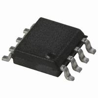
HCPL-0708-560E Avago Technologies US Inc., HCPL-0708-560E Datasheet - Page 6

HCPL-0708-560E
Manufacturer Part Number
HCPL-0708-560E
Description
OPTOCOUPLER 15MBD VDE 8-SOIC
Manufacturer
Avago Technologies US Inc.
Datasheet
1.HCPL-0708-500E.pdf
(12 pages)
Specifications of HCPL-0708-560E
Package / Case
8-SOIC (0.154", 3.90mm Width)
Voltage - Isolation
3750Vrms
Number Of Channels
1, Unidirectional
Current - Output / Channel
2mA
Data Rate
15MBd
Propagation Delay High - Low @ If
35ns @ 12mA
Current - Dc Forward (if)
20mA
Input Type
DC
Output Type
Push-Pull, Totem-Pole
Mounting Type
Surface Mount
Isolation Voltage
3750 Vrms
Maximum Continuous Output Current
2 mA
Maximum Fall Time
25 ns
Maximum Forward Diode Current
20 mA
Maximum Rise Time
20 ns
Minimum Forward Diode Voltage
1.3 V
Output Device
Logic Gate Photo IC
Configuration
1 Channel
Maximum Baud Rate
15 MBps
Maximum Forward Diode Voltage
1.8 V
Maximum Operating Temperature
+ 100 C
Minimum Operating Temperature
- 40 C
Lead Free Status / RoHS Status
Lead free / RoHS Compliant
Available stocks
Company
Part Number
Manufacturer
Quantity
Price
Company:
Part Number:
HCPL-0708-560E
Manufacturer:
AVAGO
Quantity:
40 000
IEC/EN/DIN EN 60747-5-2 Insulation Related Characteristics (Option 060)
†Refer to the front of the optocoupler section of the Isolation and Control Component Designer’s Catalog, under Product Safety Regulations sec-
tion IEC/EN/DIN EN 60747-5-2, for a detailed description.
Recommended Operating Conditions
Absolute Maximum Ratings
Description
Installation classification per DIN VDE 0110/1.89, Table 1
Climatic Classification
Pollution Degree (DIN VDE 0110/1.89)
Maximum Working Insulation Voltage
Input to Output Test Voltage, Method b†
Input to Output Test Voltage, Method a†
Highest Allowable Overvoltage†
(Transient Overvoltage, t
Safety Limiting Values
Insulation Resistance at T
Parameter
Ambient Operating Temperature
Supply Voltages
Input Current (ON)
Parameter
Storage Temperature
Ambient Operating Temperature
Supply Voltages
Output Voltage
Average Output Current
Average Forward Input Current
Lead Solder Temperature
Solder Reflow Temperature Profile
V
Test with t
V
for rated mains voltage ≤150 V rms
for rated mains voltage ≤300 V rms
for rated mains voltage ≤450 V rms
t
(Maximum values allowed in the event of a failure,
also see Thermal Derating curve, Figure 11.)
m
IORM
IORM
Case Temperature
Input Current
Output Power
= 60 sec, Partial Discharge < 5 pC
x 1.875 = V
x 1.5 = V
m
= 1 sec, Partial Discharge < 5 pC
PR
, Type and Sample Test,
PR
, 100% Production
ini
S
, V
= 10 sec)
10
= 500 V
[1]
Symbol
T
T
V
V
I
I
O
F
A
S
O
DD
Symbol
T
V
I
F
A
DD
See Solder Reflow Temperature Profile Section
260°C for 10 sec., 1.6 mm below seating plane
Min.
–55
–40
0
–0.5
Symbol
V
V
V
V
T
I
P
R
S,INPUT
IORM
S
S,OUTPUT
IO
PR
PR
IOTM
Min.
–40
4.5
10
Max.
125
+100
6
V
2
20
DD2
+0.5
HCPL-0708 Option 060
I-IV
I-III
55/85/21
2
560
1050
840
4000
150
150
600
≥10
9
Max.
+100
5.5
16
Units
°C
°C
Volts
Volts
mA
mA
Units
°C
V
mA
Figure
Units
V peak
V peak
V peak
V peak
°C
mA
mW
Ω
Figure
1, 2


