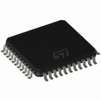
L6710 STMicroelectronics, L6710 Datasheet - Page 9

L6710
Manufacturer Part Number
L6710
Description
IC CTRLR 6BIT 2PH PROGR 44-TQFP
Manufacturer
STMicroelectronics
Type
Step-Down (Buck)r
Datasheet
1.L6710.pdf
(34 pages)
Specifications of L6710
Internal Switch(s)
No
Synchronous Rectifier
Yes
Number Of Outputs
2
Voltage - Output
0.84 ~ 1.6 V
Current - Output
2A
Frequency - Switching
150kHz
Voltage - Input
12V
Operating Temperature
0°C ~ 125°C
Mounting Type
Surface Mount
Package / Case
44-TQFP, 44-VQFP
Power - Output
2.5W
Product
Half-Bridge Drivers
Supply Current
12.5 mA
Mounting Style
SMD/SMT
Lead Free Status / RoHS Status
Lead free / RoHS Compliant
Available stocks
Company
Part Number
Manufacturer
Quantity
Price
Company:
Part Number:
L671000
Manufacturer:
PHI
Quantity:
1 870
Part Number:
L671000
Manufacturer:
OKI
Quantity:
20 000
OSCILLATOR
The switching frequency is internally fixed at 150kHz. Each phase works at the frequency fixed by the os-
cillator so that the resulting switching frequency at the load side results in being doubled.
The internal oscillator generates the triangular waveform for the PWM charging and discharging with a
constant current an internal capacitor. The current delivered to the oscillator is typically 25µA
(Fsw=150kHz) and may be varied using an external resistor (R
GND or Vcc. Since the OSC pin is maintained at fixed voltage (Typ. 1.237V), the frequency is varied pro-
portionally to the current sunk (forced) from (into) the pin considering the internal gain of 6KHz/µA.
In particular connecting it to GND the frequency is increased (current is sunk from the pin), while connect-
ing R
relationships:
Note that forcing 25µA into this pin, the device stops switching because no current is delivered to the os-
cillator.
Figure 1. R
DIGITAL TO ANALOG CONVERTER AND REFERENCE
The built-in digital to analog converter allows the adjustment of the output voltage from 0.8375V to
1.6000V with 12.5mV as shown in the previous table 1 automatically regulating VID* = VID - 25mV in order
to avoid any external component or circuitry to lower the regulated voltage meeting VRD10 specs. The
internal reference is trimmed to ensure the output voltage precision of ±0.5% and a zero temperature co-
efficient around 70°C. The internal reference voltage for the regulation is programmed by the voltage iden-
tification (VID) pins. These are inputs of an internal DAC that is realized by means of a series of resistors
providing a partition of the internal voltage reference. The VID code drives a multiplexer that selects a volt-
age on a precise point of the divider. The DAC output is delivered to an amplifier obtaining the V
age reference (i.e. the set-point of the error amplifier). Internal pull-ups are provided (realized with a 5µA
current generator up to 3V Typ); in this way, to program a logic "1" it is enough to leave the pin floating,
while to program a logic "0" it is enough to short the pin to GND. Programming the "11111x" code (VID5
doesn't matter), the device enters the NOCPU mode: all mosfets are turned OFF.
OSC
14000
12000
10000
to Vcc=12V the frequency is reduced (current is forced into the pin), according to the following
8000
6000
4000
2000
OSC
0
25
vs. Switching Frequency
ROSC vs. GND:
ROSC vs. 12V:
50
Frequency (KHz)
75
100
f
S
f
S
=
=
150KHz
150KHz
125
150
+
+
12 1.237
------------------------ - 6 kHz
-------------- - 6 kHz
R
1.237
R
O SC
–
OS C
⋅
---------- -
⋅
µA
---------- -
800
700
600
500
400
300
200
100
µA
=
0
150
150kHz
=
OSC
150kHz
) connected between OSC pin and
250
+
-----------------------------
R
7.422 10
Frequency (KHz)
+
O SC
-----------------------------
R
6.457 10
350
O SC
(
⋅
KΩ
(
⋅
KΩ
6
)
450
7
)
550
PROG
650
L6710
volt-
9/34


