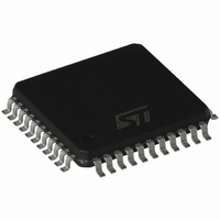
L6710 STMicroelectronics, L6710 Datasheet - Page 23

L6710
Manufacturer Part Number
L6710
Description
IC CTRLR 6BIT 2PH PROGR 44-TQFP
Manufacturer
STMicroelectronics
Type
Step-Down (Buck)r
Datasheet
1.L6710.pdf
(34 pages)
Specifications of L6710
Internal Switch(s)
No
Synchronous Rectifier
Yes
Number Of Outputs
2
Voltage - Output
0.84 ~ 1.6 V
Current - Output
2A
Frequency - Switching
150kHz
Voltage - Input
12V
Operating Temperature
0°C ~ 125°C
Mounting Type
Surface Mount
Package / Case
44-TQFP, 44-VQFP
Power - Output
2.5W
Product
Half-Bridge Drivers
Supply Current
12.5 mA
Mounting Style
SMD/SMT
Lead Free Status / RoHS Status
Lead free / RoHS Compliant
Available stocks
Company
Part Number
Manufacturer
Quantity
Price
Company:
Part Number:
L671000
Manufacturer:
PHI
Quantity:
1 870
Part Number:
L671000
Manufacturer:
OKI
Quantity:
20 000
Figure 16. Power connections and related connections layout guidelines (same for both phases).
– Power Connections.
These are the connections where switching and continuous current flows from the input supply towards
the load. The first priority when placing components has to be reserved to this power section, minimizing
the length of each connection and loop as much as possible. To minimize noise and voltage spikes (EMI
and losses) these interconnections must be a part of a power plane and anyway realized by wide and thick
copper traces: loop must be anyway minimized. The critical components, i.e. the power transistors, must
be located as close as possible one to the other.
Fig. 16a shows the details of the power connections involved and the current loops. The input capacitance
(C
order to eliminate the stray inductance generated by the copper traces. Low ESR and ESL capacitors are
required.
Use as much VIAs as possible when power traces have to move between different planes on the PCB:
this reduces both parasitic resistance and inductance. Moreover, reproducing the same high-current trace
on more than one PCB layer will reduce the parasitic resistance associated to that connection.
Connect output bulk capacitor as near as possible to the load, minimizing parasitic inductance and resis-
tance associated to the copper trace also adding extra decoupling capacitors along the way to the load
when this results in being far from the bulk capacitor bank.
– Power Connections Related.
Fig.16b shows some small signal components placement, and how and where to mix signal and power
ground planes. The distance from drivers and mosfet gates should be reduced as much as possible. Prop-
agation delay times as well as for the voltage spikes generated by the distributed inductance along the
copper traces are so minimized.
In fact, the further the mosfet is from the device, the longer is the interconnecting gate trace and as a con-
sequence, the higher are the voltage spikes corresponding to the gate PWM rising and falling signals.
Even if these spikes are clamped by inherent internal diodes, propagation delays, noise and potential
causes of instabilities are introduced jeopardizing good system behavior. One important consequence is
that the switching losses for the high side mosfet are significantly increased.
For this reason, it is suggested to have the device oriented with the driver side towards the mosfets and
the GATEx and PHASEx traces walking together toward the high side mosfet in order to minimize distance
(see fig 17). In addition, since the PHASEx pin is the return path for the high side driver, this pin must be
connected directly to the High Side mosfet Source pin to have a proper driving for this mosfet.
For the LS mosfets, the return path is the PGND pin: it can be connected directly to the power ground
plane (if implemented) or in the same way to the LS mosfets Source pin. GATEx and PHASEx connections
(and also PGND when no power ground plane is implemented) must also be designed to handle current
peaks in excess of 2A (30 mils wide is suggested).
IN
), or at least a portion of the total capacitance needed, has to be placed close to the power section in
HGATEx
PHASEx
LGATEx
PGNDx
a. PCB power and ground planes areas
R
R
gate
gate
HS
LS
D
V
C
IN
IN
L
C
OUT
LOAD
SGND
b. PCB small signal components placement
PHASEx
BOOTx
VCC
C
BOOTx
+V
CC
C
VCC
HS
LS
D
V
C
IN
IN
L
C
OUT
LOAD
L6710
23/34


