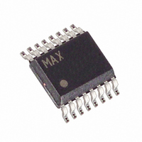
MAX1653EEE Maxim Integrated Products, MAX1653EEE Datasheet - Page 25

MAX1653EEE
Manufacturer Part Number
MAX1653EEE
Description
IC CTRLR DCDC PWM STPDWN 16-QSOP
Manufacturer
Maxim Integrated Products
Type
Step-Down (Buck)r
Datasheet
1.MAX1655ESE.pdf
(28 pages)
Specifications of MAX1653EEE
Internal Switch(s)
No
Synchronous Rectifier
Yes
Number Of Outputs
1
Voltage - Output
2.5 ~ 5.5 V
Current - Output
10A
Frequency - Switching
150kHz, 300kHz
Voltage - Input
4.5 ~ 30 V
Operating Temperature
-40°C ~ 85°C
Mounting Type
Surface Mount
Package / Case
16-QSOP
Power - Output
667mW
Output Voltage
2.5 V to 5.5 V
Output Current
10 A
Input Voltage
4.5 V to 30 V
Mounting Style
SMD/SMT
Maximum Operating Temperature
+ 85 C
Minimum Operating Temperature
- 40 C
Lead Free Status / RoHS Status
Contains lead / RoHS non-compliant
Available stocks
Company
Part Number
Manufacturer
Quantity
Price
Company:
Part Number:
MAX1653EEE
Manufacturer:
MAXIM
Quantity:
35
Part Number:
MAX1653EEE
Manufacturer:
MAXIM/美信
Quantity:
20 000
Part Number:
MAX1653EEE+
Manufacturer:
MAXIM/美信
Quantity:
20 000
Company:
Part Number:
MAX1653EEE+T
Manufacturer:
MAXIM
Quantity:
9
2) Place the IC and signal components. Keep the main
3) Employ a single-point star ground where the input
TOP VIEW
( ) ARE FOR MAX1652/ MAX1654.
of top-layer copper, so that they don’t go through
vias. The resulting top-layer “sub-ground-plane” is
connected to the normal inner-layer ground plane at
the output ground terminals. This ensures that the
analog GND of the IC is sensing at the output termi-
nals of the supply, without interference from IR
drops and ground noise. Other high-current paths
should also be minimized, but focusing ruthlessly
on short ground and current-sense connections
eliminates about 90% of all PC board layout diffi-
culties. See the evaluation kit PC board layouts for
examples.
switching node (LX node) away from sensitive ana-
log components (current-sense traces and REF and
SS capacitors). Placing the IC and analog compo-
nents on the opposite side of the board from the
power-switching node is desirable. Important: the
IC must be no farther than 10mm from the current-
sense resistor. Keep the gate-drive traces (DH, DL,
and BST) shorter than 20mm and route them away
from CSH, CSL, REF, and SS.
ground trace, power ground (subground plane),
and normal ground plane all meet at the output
ground terminal of the supply.
(SECFB) SKIP
SHDN
SYNC
GND
CSH
REF
SS
FB
______________________________________________________________________________________
1
2
3
4
5
6
7
8
MAX1652
MAX1653
MAX1654
MAX1655
QSOP
DC-DC Controllers in 16-Pin QSOP
High-Efficiency, PWM, Step-Down
16
15
14
13
12
11
10
9
DH
LX
BST
DL
PGND
VL
V+
CSL
Figure 9. Kelvin Connections for the Current-Sense Resistor
SYNC
SHDN
SKIP
GND
CSH
REF
FAT, HIGH-CURRENT TRACES
SS
FB
MAIN CURRENT PATH
1
2
3
4
5
6
7
8
MAX1652
MAX1653
MAX1654
MAX1655
Narrow SO
Pin Configurations
MAX1653
MAX1655
SENSE RESISTOR
16
15
14
13
12
11
10
9
DH
LX
BST
VL
V+
CSL
DL
PGND
25


