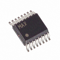
MAX1653EEE Maxim Integrated Products, MAX1653EEE Datasheet - Page 17

MAX1653EEE
Manufacturer Part Number
MAX1653EEE
Description
IC CTRLR DCDC PWM STPDWN 16-QSOP
Manufacturer
Maxim Integrated Products
Type
Step-Down (Buck)r
Datasheet
1.MAX1655ESE.pdf
(28 pages)
Specifications of MAX1653EEE
Internal Switch(s)
No
Synchronous Rectifier
Yes
Number Of Outputs
1
Voltage - Output
2.5 ~ 5.5 V
Current - Output
10A
Frequency - Switching
150kHz, 300kHz
Voltage - Input
4.5 ~ 30 V
Operating Temperature
-40°C ~ 85°C
Mounting Type
Surface Mount
Package / Case
16-QSOP
Power - Output
667mW
Output Voltage
2.5 V to 5.5 V
Output Current
10 A
Input Voltage
4.5 V to 30 V
Mounting Style
SMD/SMT
Maximum Operating Temperature
+ 85 C
Minimum Operating Temperature
- 40 C
Lead Free Status / RoHS Status
Contains lead / RoHS non-compliant
Available stocks
Company
Part Number
Manufacturer
Quantity
Price
Company:
Part Number:
MAX1653EEE
Manufacturer:
MAXIM
Quantity:
35
Part Number:
MAX1653EEE
Manufacturer:
MAXIM/美信
Quantity:
20 000
Part Number:
MAX1653EEE+
Manufacturer:
MAXIM/美信
Quantity:
20 000
Company:
Part Number:
MAX1653EEE+T
Manufacturer:
MAXIM
Quantity:
9
Table 3. Operating-Mode Truth Table
* MAX1652/MAX1654 have no SKIP pin and therefore can’t go
X = Don’t care
flow, and thereby suppresses discontinuous-mode
inductor ringing by changing the reverse current-limit
detection threshold from 0 to -100mV, allowing the
inductor current to reverse at very light loads.
In most applications, SKIP should be tied to GND in
order to minimize quiescent supply current. Supply cur-
rent with SKIP high is typically 10mA to 20mA, depend-
ing on external MOSFET gate capacitance and
switching losses.
Forced continuous conduction via SKIP can improve
cross regulation of transformer-coupled multiple-output
supplies. This second function of the SKIP pin produces
a result that is similar to the method of adding sec-
ondary regulation via the SECFB feedback pin, but with
much higher quiescent supply current. Still, improving
cross regulation by enabling SKIP instead of building in
SECFB feedback can be useful in noise-sensitive appli-
cations, since SECFB and SKIP are mutually exclusive
pins/functions in the MAX1652 family.
The MAX1652–MAX1655 family has both fixed and
adjustable output voltage modes. For fixed mode, con-
nect FB to GND for a 3.3V output and to V
SHDN
High
High
High
High
into low-noise mode.
Low
SKIP
High
Low
Low
Low
X
CURRENT
Medium,
LOAD
<10%
<30%
>30%
High,
Low,
______________________________________________________________________________________
Adjustable-Output Feedback
X
X
Low Noise*
Shutdown
MODE
(PWM)
NAME
PWM
Idle
Idle
(Dual-Mode FB Pin)
DC-DC Controllers in 16-Pin QSOP
High-Efficiency, PWM, Step-Down
All circuit blocks
turned off; supply
current = 3µA typ
Pulse-skipping;
supply current =
300µA typ at V
10V; discontinuous
inductor current
Pulse-skipping;
continuous inductor
current
Constant-frequency
PWM; continuous
inductor current
Constant-frequency
PWM regardless of
load; continuous
inductor current
even at no load
DESCRIPTION
L
for a 5V out-
IN
=
put. Adjusting the main output voltage with external
resistors is easy for any of the devices in this family, via
the circuit of Figure 6. The feedback voltage is nominal-
ly 2.5 for all family members except the MAX1655,
which has a nominal FB voltage of 1V. The output volt-
age (given by the formula in Figure 6) should be set
approximately 2% high in order to make up for the
MAX1652’s load-regulation error. For example, if
designing for a 3.0V output, use a resistor ratio that
results in a nominal output voltage of 3.06V. This slight
offsetting gives the best possible accuracy.
Recommended normal values for R5 range from 5kΩ to
100kΩ.
Remote sensing of the output voltage, while not possi-
ble in fixed-output mode due to the combined nature of
the voltage- and current-sense input (CSL), is easy to
achieve in adjustable mode by using the top of the
external resistor divider as the remote sense point.
The MAX1652/MAX1653/MAX1654’s output voltage is
adjustable down to 2.5V and the MAX1655’s output is
adjustable as low as 1V. However, the minimum duty
factor may limit the choice of operating frequency, high
input voltage, and low output voltage.
Figure 6. Adjusting the Main Output Voltage
WHERE V
V
OUT
MAX1655
MAX1652
MAX1653
MAX1654
= V
GND
REF
REF
(
(NOMINAL) = 2.5V (MAX1652–MAX1654)
1 + –––
CSH
CSL
DH
DL
R4
R5
FB
)
= 1.0V (MAX1655)
Duty-Factor Limitations for
V+
Low V
OUT
REMOTE
/V
SENSE
LINES
R5
IN
R4
Ratios
OUTPUT
MAIN
17


