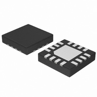
NCP5212AMNTXG ON Semiconductor, NCP5212AMNTXG Datasheet - Page 15

NCP5212AMNTXG
Manufacturer Part Number
NCP5212AMNTXG
Description
IC CTLR SYNC SGL STEPDOWN 16-QFN
Manufacturer
ON Semiconductor
Type
Step-Down (Buck)r
Datasheet
1.NCP5212AMNTXG.pdf
(19 pages)
Specifications of NCP5212AMNTXG
Internal Switch(s)
No
Synchronous Rectifier
No
Number Of Outputs
1
Voltage - Output
0.8 ~ 3.3 V
Frequency - Switching
300kHz
Voltage - Input
4.5 ~ 27 V
Operating Temperature
-40°C ~ 85°C
Mounting Type
Surface Mount
Package / Case
16-TFQFN Exposed Pad
Output Voltage
0.8 V to 3.3 V
Output Current
35 uA
Input Voltage
4.5 V to 27 V
Supply Current
35 uA
Mounting Style
SMD/SMT
Maximum Operating Temperature
+ 150 C
Minimum Operating Temperature
- 40 C
Lead Free Status / RoHS Status
Lead free / RoHS Compliant
Current - Output
-
Power - Output
-
Lead Free Status / Rohs Status
Lead free / RoHS Compliant
Available stocks
Company
Part Number
Manufacturer
Quantity
Price
Company:
Part Number:
NCP5212AMNTXG
Manufacturer:
ON Semiconductor
Quantity:
12 000
Part Number:
NCP5212AMNTXG
Manufacturer:
ON/安森美
Quantity:
20 000
programming stage at system start up. This is used to sense
the voltage level which is developed by a resistor Rocp so as
to program the overcurrent detection threshold voltage. For
typical application, the V
typ) by setting Rocp = 0 W, or directly short the IDRP/OCP
pin to ground. It has the benefit of saving one component at
application board. For other programming values of V
please refer to the electrical table of “Overcurrent Protection
Setting” section.
Guidelines for selecting OCP Trip Component
Overvoltage Protection (OVP)
voltage for over 1.5 ms blanking time, an OV fault is set. At
that moment, the top gate drive is turned off and the bottom
gate drive is turned on until the V
voltage (UV) threshold and bottom gate drive is turned on
again whenever V
When V
1. Choose the value of Rocp for V
2. Define the DC value of OCP trip point(I
3. Calculate the inductor peak current (I
4. Check with inductor datasheet to find out the value
5. Select C
6. Calculate Rs1 value by the equation:
7. Calculate Rs2 value by the equation:
8. Hence, all the current sense components Rs1, Rs2,
9. If Rs2 is not used (open), set k = 1, at that
that you want. The typical value is 1.5 to 1.8 times
of maximum loading current. For example, if
maximum loading is 10 A, then set OCP trip point
at 15 A to 18 A.
estimated by the equation:
of inductor DC resistance DCR, then calculate the
RS1, RS2 dividing factor k based on the equation:
Typically, 100 nF will be used.
Cs had been found for taget I
moment, the I
FB
I
pk
voltage is above OVPth+ of the nominal V
+ I
S
value between 100 nF to 200 nF.
FB
Rs1 +
OCP_DC
pk
goes above upper UV threshold. EN
Rs2 +
k +
I
will be restricted by:
pk
octh
k * DCR * Cs
I
+
)
pk
V
is set as default value(40 mV
k * Rs1
2 * V
V
DCR
* DCR
1 * k
V
octh
octh
o
L
* (V
IN
FB
OCP_DC
* f
IN
SW
octh
* V
below lower under
* L
selection.
o
.
)
pk
o
)which is
OCP_DC
(eq. 4)
(eq. 5)
(eq. 6)
(eq. 7)
(eq. 8)
http://onsemi.com
octh
)
FB
,
15
resets or power recycle the device can exit the fault. The
following diagram shows the typical waveform when OVP
event occurs.
Undervoltage Protection (UVP)
voltage event. The under voltage limit is 80% (typical) of the
nominal V
threshold over consecutive 8 clock cycles, an UV fault is set
and the device is latched off such that both top and bottom
gate drives are off. EN resets or power recycle the device can
exit the fault.
Thermal Shutdown
150°C. The IC restarts operation only after the junction
temperature drops below 125°C.
An UVP circuit monitors the V
The IC will shutdown if the die temperature exceeds
Figure 26. Undervoltage Protection
Figure 25. Overvoltage Protection
FB
Top to Bottom : SWN, DL, Vo, PGOOD
Top to Bottom : SWN, Vo, PGOOD
voltage. If the V
FB
FB
voltage to detect under
voltage is below this


