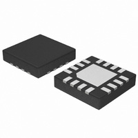
NCP5212AMNTXG ON Semiconductor, NCP5212AMNTXG Datasheet - Page 12

NCP5212AMNTXG
Manufacturer Part Number
NCP5212AMNTXG
Description
IC CTLR SYNC SGL STEPDOWN 16-QFN
Manufacturer
ON Semiconductor
Type
Step-Down (Buck)r
Datasheet
1.NCP5212AMNTXG.pdf
(19 pages)
Specifications of NCP5212AMNTXG
Internal Switch(s)
No
Synchronous Rectifier
No
Number Of Outputs
1
Voltage - Output
0.8 ~ 3.3 V
Frequency - Switching
300kHz
Voltage - Input
4.5 ~ 27 V
Operating Temperature
-40°C ~ 85°C
Mounting Type
Surface Mount
Package / Case
16-TFQFN Exposed Pad
Output Voltage
0.8 V to 3.3 V
Output Current
35 uA
Input Voltage
4.5 V to 27 V
Supply Current
35 uA
Mounting Style
SMD/SMT
Maximum Operating Temperature
+ 150 C
Minimum Operating Temperature
- 40 C
Lead Free Status / RoHS Status
Lead free / RoHS Compliant
Current - Output
-
Power - Output
-
Lead Free Status / Rohs Status
Lead free / RoHS Compliant
Available stocks
Company
Part Number
Manufacturer
Quantity
Price
Company:
Part Number:
NCP5212AMNTXG
Manufacturer:
ON Semiconductor
Quantity:
12 000
Part Number:
NCP5212AMNTXG
Manufacturer:
ON/安森美
Quantity:
20 000
General
power controller contains a PWM controller for wide
battery/adaptor voltage range applications
monitor, soft−start, overcurrent protection, undervoltage
protection, overvoltage protection and thermal shutdown.
The NCP5212A/NCP5212T features power saving function
which can increase the efficiency at light load. It is ideal for
battery operated systems. The IC is packaged in QFN16.
Control Logic
is controlled by an EN pin. The EN pin serves two functions.
When voltage of EN is below VEN_Disable, it shuts down
the device. When the voltage of EN is at the level of
VEN_Master, the device is operating as Master mode. When
voltage level of EN is at VEN_Slave, the device is operating
as Slave mode. It should be noted that no matter the device
is operating either at Master or Slave mode, the device is
operating in the manner of auto power saving condition such
that it operates as skip mode automatically at light load.
When EN is above VEN_Disable, the internal V
activated and power−on reset occurs which resets all the
protection faults. Once V
internal signal will wake up the supply undervoltage
monitor which will assert a “GOOD” condition. In addition,
the NCP5212A/NCP5212T continuously monitors V
V
Single Device Operation
the SYNC pin is pull to ground. Under this configuration, the
device will use the internal clock for normal PWM
operation.
Dual Device Operation (Master/Salve Mode)
devices are tied up together. (Detail configuration please see
the application schematic) One device is served as Master
and another one is served as Slave. Once they already, they
are synchronized to each other and they are operating as
“interleaved” mode such that the phase shift of their
switching clocks is 180°. It has the benefit that the amount
of ripple current at the V
bulk capacitors at V
material cost. Figure 15 and Figure 16 show the difference
when
(unsynchronized) and operating at interleaved mode
(Synchronized). It can be seen that at the unsynchronized
condition, the system is obviously noisy because of high
ripple voltage at V
amount of ripple current at V
operating at interleaving mode, the overall V
current is significantly reduced.
IN
The NCP5212A/NCP5212T synchronous stepdown
The NCP5212A/NCP5212T includes power good voltage
The internal control logic is powered by V
The device is operating as single device operation when
The device is operating as Master/Slave mode if two
levels with undervoltage lockout (UVLO) function.
the
devices
IN
IN
to save the confined PCB space and
(ripple voltage directly reflects the
ref
IN
are
reaches its regulation voltage, an
will be lower and hence lesser
IN
operating
). Once the devices are
DETAILED OPERATING DESCRIPTION
CC
independently
. The device
IN
http://onsemi.com
CC
ripple
ref
and
is
12
Transient Response Enhancement (TRE)
response time is one switching cycle in the worst case. To
further improve transient response in CCM, a transient
response enhancement circuitry is implemented inside the
NCP5212A/NCP5212T. In CCM operation, the controller is
continuously monitoring the COMP pin output voltage of
the error amplifier to detect the load transient events. The
functional block diagram of TRE is shown below.
Figure 16. Two Devices are in Interleaved Operation
For the conventional PWM controller in CCM, the fastest
Top to Bottom: VIN AC Voltage, SWN_Slave, SWN_Master
Top to Bottom: VIN AC Voltage, SWN_Slave, SWN_Master
Figure 15. Two Devices are Unsynchronized
Figure 17. Block Diagram of TRE Circuit
internal TRE_TH
COMP
R
C
+
+
TRE


