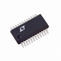
LTC1436AIGN Linear Technology, LTC1436AIGN Datasheet - Page 7

LTC1436AIGN
Manufacturer Part Number
LTC1436AIGN
Description
IC SW REG SYNC STEP-DOWN 24-SSOP
Manufacturer
Linear Technology
Type
Step-Down (Buck)r
Datasheet
1.LTC1436AIGN-PLLPBF.pdf
(28 pages)
Specifications of LTC1436AIGN
Internal Switch(s)
No
Synchronous Rectifier
Yes
Number Of Outputs
1
Voltage - Output
1.19 ~ 9 V
Current - Output
50mA
Frequency - Switching
125kHz ~ 240kHz
Voltage - Input
3.5 ~ 30 V
Operating Temperature
-40°C ~ 85°C
Mounting Type
Surface Mount
Package / Case
24-SSOP
Lead Free Status / RoHS Status
Contains lead / RoHS non-compliant
Power - Output
-
Available stocks
Company
Part Number
Manufacturer
Quantity
Price
Part Number:
LTC1436AIGN#PBF
Manufacturer:
LINEAR/凌特
Quantity:
20 000
Company:
Part Number:
LTC1436AIGN-PLL
Manufacturer:
Linear Technology
Quantity:
135
Part Number:
LTC1436AIGN-PLL
Manufacturer:
LT/凌特
Quantity:
20 000
Part Number:
LTC1436AIGN-PLL#PBF
Manufacturer:
LINEAR/凌特
Quantity:
20 000
PIN
TYPICAL PERFORMANCE CHARACTERISTICS
V
IC’s signal ground pin.
INTV
Switch. The driver and control circuits are powered from
this voltage. Must be closely decoupled to power ground
with a minimum of 2.2µF tantalum or electrolytic capacitor.
DRV
EXTV
This switch closes and supplies V
EXTV
Applications Information section. Do not exceed 10V on
this pin. Connect to V
BOOST: Supply to Topside Floating Driver. The bootstrap
capacitor is returned to this pin. Voltage swing at this pin
is from INTV
SW: Switch Node Connection to Inductor. Voltage swing
at this pin is from a Schottky diode (external) voltage drop
below ground to V
SGND: Small Signal Ground. Must be routed separately
from other grounds to the (–) terminal of C
PGND: Driver Power Ground. Connects to source of
bottom N-channel MOSFET and the (–) terminal of C
IN
20
15
10
U
5
0
: Main Supply Pin. Must be closely decoupled to the
CC
0
Auxiliary Regulator
Sink Current Available
CC
CC
CC
FUNCTIONS
: Bottom MOSFET Driver Supply Voltage.
: Output of the Internal 5V Regulator and EXTV
: Input to the Internal Switch Connected to INTV
2
is higher than 4.7V. See EXTV
U
4
CC
AUX DR VOLTAGE (V)
6
to V
IN
8
IN
.
U
OUT
10
+ INTV
if V
12
W
OUT
CC
14
1436 G19
.
U
≥ 5V.
16
CC
CC
power whenever
70
60
50
40
30
20
10
10
connection in
Auxiliary Regulator PSRR
OUT
.
FREQUENCY (kHz)
IN
CC
CC
.
.
100
10mA LOAD
100mA LOAD
SENSE
SENSE
in offsets between SENSE
with R
V
either from the output or from an external resistive divider
across the output . The V
V
V
< V
connected to the output. With V
output is set to 5V with V
Leaving V
set by an external resistive divider connected to V
C
the operating frequency.
I
comparator threshold increases with this control voltage.
Nominal voltage range for this pin is 0V to 2.5V.
RUN/SS: Combination of Soft Start and Run Control
Inputs. A capacitor to ground at this pin sets the ramp time
to full current output. The time is approximately 0.5s/µF.
TH
OSENSE
OSENSE
PROG
OSC
: Error Amplifier Compensation Point. The current
INTVCC
: External capacitor C
: This voltage selects the output voltage. For V
SENSE
–
+
: Receives the remotely sensed feedback voltage
: The (–) Input to the Current Comparator.
: The (+) Input to the Current Comparator. Built-
1436 G20
must connect to.
PROG
/3 the output is set to 3.3V with V
1000
LTC1436A-PLL/LTC1437A
set the current trip thresholds.
open (DC) allows the output voltage to be
100
80
95
90
85
75
70
65
60
55
50
0.001
Efficiency and Power Loss vs
Load Current
V
V
R
IN
OUT
SENSE
= 10V
PROG
–
OSENSE
= 5V
OSC
and SENSE
= 0.033Ω
EFFICIENCY
0.01
LOAD CURRENT (A)
from this pin to ground sets
pin determines which point
connected to the output.
PROG
0.1
+
pins in conjunction
> V
LTC1436A
POWER LOSS
INTVCC
1
1436 G21
/1.5 the
OSENSE
10
OSENSE
100
10
1
0.1
0.01
0.001
14367afb
PROG
7
.


