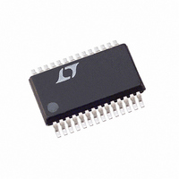
LTC3729EG Linear Technology, LTC3729EG Datasheet - Page 8

LTC3729EG
Manufacturer Part Number
LTC3729EG
Description
IC SW REG SYNC STEP-DOWN 28-SSOP
Manufacturer
Linear Technology
Series
PolyPhase®r
Type
Step-Down (Buck)r
Datasheet
1.LTC3729EGPBF.pdf
(30 pages)
Specifications of LTC3729EG
Internal Switch(s)
No
Synchronous Rectifier
Yes
Number Of Outputs
1
Voltage - Output
0.8 ~ 5 V
Current - Output
5A
Frequency - Switching
1.1MHz
Voltage - Input
4 ~ 36 V
Operating Temperature
-40°C ~ 85°C
Mounting Type
Surface Mount
Package / Case
28-SSOP
Lead Free Status / RoHS Status
Contains lead / RoHS non-compliant
Power - Output
-
Available stocks
Company
Part Number
Manufacturer
Quantity
Price
Part Number:
LTC3729EG#PBF
Manufacturer:
LINEAR/凌特
Quantity:
20 000
Company:
Part Number:
LTC3729EGN
Manufacturer:
PHILIPS
Quantity:
15
LTC3729
PIN FUNCTIONS
RUN/SS (Pin 1/Pin 28): Combination of Soft‑Start, Run
Control Input and Short‑Circuit Detection Timer. A capaci‑
tor to ground at this pin sets the ramp time to full current
output. Forcing this pin below 0.8V causes the IC to shut
down all internal circuitry. All functions are disabled in
shutdown.
SENSE1
pin voltage and built‑in offsets between SENSE
SENSE
trip threshold.
SENSE1
Input to the Differential Current Comparators.
EAIN (Pin 4/Pin 1): Input to the Error Amplifier that com‑
pares the feedback voltage to the internal 0.8V reference
voltage. This pin is normally connected to a resistive divider
from the output of the differential amplifier (DIFFOUT).
PLLFLTR (Pin 5/Pin 2): The Phase‑Locked Loop’s Low
Pass Filter is tied to this pin. Alternatively, this pin can
be driven with an AC or DC voltage source to vary the
frequency of the internal oscillator.
PLLIN (Pin 6/Pin 3): External Synchronization Input to
Phase Detector. This pin is internally terminated to SGND
with 50kΩ. The phase‑locked loop will force the rising
top gate signal of controller 1 to be synchronized with
the rising edge of the PLLIN signal.
PHASMD (Pin 7/Pin 4): Control Input to Phase Selector
which determines the phase relationships between control‑
ler 1, controller 2 and the CLKOUT signal.
I
Regulator Compensation Point. Both current comparator’s
thresholds increase with this control voltage. The normal
voltage range of this pin is from 0V to 2.4V.
SGND (Pin 9/Pin 6): Signal Ground, common to both con‑
trollers, must be routed separately from the input switched
current ground path to the common (–) terminal(s) of the
C
8
TH
Input to the Differential Current Comparators. The I
OUT
(Pin 8/Pin 5): Error Amplifier Output and Switching
capacitor(s).
+
+
–
pins in conjunction with R
, SENSE2
, SENSE2
–
+
(Pins 3, 13/Pins 31, 11): The (–)
(Pins 2,14/Pins 30, 12): The (+)
G Package/UH Package
SENSE
set the current
–
and
TH
V
that provides true remote output voltage sensing. This pin
normally drives an external resistive divider that sets the
output voltage.
V
Amplifier. Internal precision resistors capable of being
electronically switched in or out can configure it as a dif‑
ferential amplifier or an uncommitted Op Amp.
PGOOD (Pin 15/Pin 13): Open‑Drain Logic Output. PGOOD
is pulled to ground when the voltage on the EAIN pin is
not within ±7.5% of its set point.
TG2, TG1 (Pins 16, 27/Pins 14, 26): High Current Gate
Drives for Top N‑Channel MOSFETS. These are the outputs
of floating drivers with a voltage swing equal to INTV
superimposed on the switch node voltage SW.
SW2, SW1 (Pins 17, 26/Pins 15, 25): Switch Node
Connections to Inductors. Voltage swing at these pins
is from a Schottky diode (external) voltage drop below
ground to V
BOOST2, BOOST1 (Pins 18, 25/Pins 17, 24): Bootstrapped
Supplies to the Topside Floating Drivers. Capacitors
are connected between the Boost and Switch pins and
Schottky diodes are tied between the Boost and INTV
pins. Voltage swing at the Boost pins is from INTV
(V
BG2, BG1 (Pins 19, 23/Pins 18, 22): High Current Gate
Drives for Bottom Synchronous N‑Channel MOSFETS.
Voltage swing at these pins is from ground to INTV
PGND (Pin 20/Pin 19): Driver Power Ground. Connect
to sources of bottom N‑channel MOSFETS and the (–)
terminals of C
INTV
Low Dropout Regulator and the EXTV
and control circuits are powered from this voltage source.
Decouple to power ground with a 1µF ceramic capacitor
placed directly adjacent to the IC and minimum of 4.7µF
additional tantalum or other low ESR capacitor.
DIFFOUT
OS
IN
–
, V
+ INTV
CC
OS
(Pin 21/Pin 20): Output of the Internal 5V Linear
(Pin 10/Pin 7): Output of a Differential Amplifier
+
(Pins 11, 12/Pins 8, 9): Inputs to an Operational
CC
IN
.
).
IN
.
CC
Switch. The driver
CC
CC
3729fb
.
CC
CC
to


