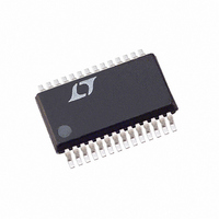
LTC3729EG Linear Technology, LTC3729EG Datasheet - Page 13

LTC3729EG
Manufacturer Part Number
LTC3729EG
Description
IC SW REG SYNC STEP-DOWN 28-SSOP
Manufacturer
Linear Technology
Series
PolyPhase®r
Type
Step-Down (Buck)r
Datasheet
1.LTC3729EGPBF.pdf
(30 pages)
Specifications of LTC3729EG
Internal Switch(s)
No
Synchronous Rectifier
Yes
Number Of Outputs
1
Voltage - Output
0.8 ~ 5 V
Current - Output
5A
Frequency - Switching
1.1MHz
Voltage - Input
4 ~ 36 V
Operating Temperature
-40°C ~ 85°C
Mounting Type
Surface Mount
Package / Case
28-SSOP
Lead Free Status / RoHS Status
Contains lead / RoHS non-compliant
Power - Output
-
Available stocks
Company
Part Number
Manufacturer
Quantity
Price
Part Number:
LTC3729EG#PBF
Manufacturer:
LINEAR/凌特
Quantity:
20 000
Company:
Part Number:
LTC3729EGN
Manufacturer:
PHILIPS
Quantity:
15
APPLICATIONS INFORMATION
Accepting larger values of ∆I
ductances, but can result in higher output voltage ripple.
A reasonable starting point for setting ripple current is
∆I
I
∆I
inductor ripple currents are constant determined by the
inductor, input and output voltages.
Inductor Core Selection
Once the values for L1 and L2 are known, the type of
inductor must be selected. High efficiency converters
generally cannot afford the core loss found in low cost
powdered iron cores, forcing the use of more expensive
ferrite, molypermalloy, or Kool Mµ
is independent of core size for a fixed inductor value, but it
is very dependent on inductance selected. As inductance
increases, core losses go down. Unfortunately, increased
inductance requires more turns of wire and therefore cop‑
per losses will increase.
Ferrite designs have very low core loss and are preferred
at high switching frequencies, so design goals can con‑
centrate on copper loss and preventing saturation. Ferrite
core material saturates “hard,” which means that induc‑
tance collapses abruptly when the peak design current is
exceeded. This results in an abrupt increase in inductor
Kool Mµ is a registered trademark of Magnetics, Inc.
OUT
L
L
= 0.4(I
occurs at the maximum input voltage. The individual
is the total load current. Remember, the maximum
Figure 3. Normalized Peak Output Current vs
Duty Factor [I
OUT
)/N, where N is the number of channels and
1.0
0.9
0.8
0.7
0.6
0.5
0.4
0.3
0.2
0.1
0
0.1
RMS
0.2
≈ 0.3 (∆I
0.3
DUTY FACTOR (V
0.4
O(P–P)
L
0.5
allows the use of low in‑
®
)]
cores. Actual core loss
OUT
0.6
/V
IN
0.7
1-PHASE
2-PHASE
3-PHASE
4-PHASE
6-PHASE
)
0.8
3729
F03
0.9
ripple current and consequent output voltage ripple. Do
not allow the core to saturate!
Molypermalloy (from Magnetics, Inc.) is a very good, low
loss core material for toroids, but it is more expensive
than ferrite. A reasonable compromise from the same
manufacturer is Kool Mµ. Toroids are very space effi‑
cient, especially when you can use several layers of wire.
Because they lack a bobbin, mounting is more difficult.
However, designs for surface mount are available which
do not increase the height significantly.
Power MOSFET, D1 and D2 Selection
Two external power MOSFETs must be selected for each
controller with the LTC3729: One N‑channel MOSFET for
the top (main) switch, and one N‑channel MOSFET for the
bottom (synchronous) switch.
The peak‑to‑peak drive levels are set by the INTV
This voltage is typically 5V during start‑up (see EXTV
Connection). Consequently, logic‑level threshold MOSFETs
must be used in most applications. The only exception
is if low input voltage is expected (V
logic‑level threshold MOSFETs (V
used. Pay close attention to the BV
the MOSFETs as well; most of the logic‑level MOSFETs
are limited to 30V or less.
Selection criteria for the power MOSFETs include the
“ON” resistance R
C
the LTC3729 is operating in continuous mode the duty
factors for the top and bottom MOSFETs of each output
stage are given by:
The MOSFET power dissipations at maximum output
current are given by:
RSS
Main Switch Duty Cycle =
Synchronous Switch Duty Cycle =
, input voltage, and maximum output current. When
DS(ON)
, reverse transfer capacitance
V
V
OUT
IN
GS(TH)
DSS
IN
LTC3729
V
< 5V); then, sub‑
specification for
< 3V) should be
IN
– V
V
IN
CC
OUT
voltage.
13
CC
3729fb
Pin


