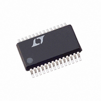
LTC3729EG Linear Technology, LTC3729EG Datasheet - Page 24

LTC3729EG
Manufacturer Part Number
LTC3729EG
Description
IC SW REG SYNC STEP-DOWN 28-SSOP
Manufacturer
Linear Technology
Series
PolyPhase®r
Type
Step-Down (Buck)r
Datasheet
1.LTC3729EGPBF.pdf
(30 pages)
Specifications of LTC3729EG
Internal Switch(s)
No
Synchronous Rectifier
Yes
Number Of Outputs
1
Voltage - Output
0.8 ~ 5 V
Current - Output
5A
Frequency - Switching
1.1MHz
Voltage - Input
4 ~ 36 V
Operating Temperature
-40°C ~ 85°C
Mounting Type
Surface Mount
Package / Case
28-SSOP
Lead Free Status / RoHS Status
Contains lead / RoHS non-compliant
Power - Output
-
Available stocks
Company
Part Number
Manufacturer
Quantity
Price
Part Number:
LTC3729EG#PBF
Manufacturer:
LINEAR/凌特
Quantity:
20 000
Company:
Part Number:
LTC3729EGN
Manufacturer:
PHILIPS
Quantity:
15
APPLICATIONS INFORMATION
LTC3729
The diagram in Figure 9 illustrates all branch currents in
a 2‑phase switching regulator. It becomes very clear after
studying the current waveforms why it is critical to keep
the high‑switching‑current paths to a small physical size.
High electric and magnetic fields will radiate from these
“loops” just as radio stations transmit signals. The output
capacitor ground should return to the negative terminal of
the input capacitor and not share a common ground path
with any switched current paths. The left half of the circuit
gives rise to the “noise” generated by a switching regulator.
The ground terminations of the sychronous MOSFETs and
Schottky diodes should return to the bottom plate(s) of the
24
R
IN
V
IN
C
IN
BOLD LINES INDICATE
HIGH, SWITCHING
CURRENT LINES.
KEEP LINES TO A
MINIMUM LENGTH.
+
Figure 9. Instantaneous Current Path Flow in a Multiple Phase Switching Regulator
SW1
SW2
D1
D2
L1
L2
input capacitor(s) with a short isolated PC trace since very
high switched currents are present. A separate isolated
path from the bottom plate(s) of the input capacitor(s)
should be used to tie in the IC power ground pin (PGND)
and the signal ground pin (SGND). This technique keeps
inherent signals generated by high current pulses from
taking alternate current paths that have finite impedances
during the total period of the switching regulator. External
OPTI‑LOOP compensation allows overcompensation for
PC layouts which are not optimized but this is not the
recommended design procedure.
R
R
SENSE1
SENSE2
+
C
V
OUT
OUT
3729
F09
R
L
3729fb


