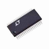
LTC1709EG#TRPBF Linear Technology, LTC1709EG#TRPBF Datasheet - Page 19

LTC1709EG#TRPBF
Manufacturer Part Number
LTC1709EG#TRPBF
Description
IC SW REG STEP-DOWN SYNC 36-SSOP
Manufacturer
Linear Technology
Type
Step-Down (Buck)r
Datasheet
1.LTC1709EG.pdf
(28 pages)
Specifications of LTC1709EG#TRPBF
Internal Switch(s)
No
Synchronous Rectifier
Yes
Number Of Outputs
2
Voltage - Output
1.3 ~ 3.5 V
Current - Output
3A
Voltage - Input
4 ~ 36 V
Operating Temperature
-40°C ~ 85°C
Mounting Type
Surface Mount
Package / Case
36-SSOP
Lead Free Status / RoHS Status
Lead free / RoHS Compliant
Power - Output
-
Frequency - Switching
-
Available stocks
Company
Part Number
Manufacturer
Quantity
Price
APPLICATIO S I FOR ATIO
Figure 6, eliminates any extra supply current during shut-
down while eliminating the INTV
ing controller start-up.
Why should you defeat current latchoff? During the
prototyping stage of a design, there may be a problem with
noise pickup or poor layout causing the protection circuit
to latch off the controller. Defeating this feature allows
troubleshooting of the circuit and PC layout. The internal
short-circuit and foldback current limiting still remains
active, thereby protecting the power supply system from
failure. A decision can be made after the design is com-
plete whether to rely solely on foldback current limiting or
to enable the latchoff feature by removing the pull-up
resistor.
The value of the soft-start capacitor C
scaled with output voltage, output capacitance and load
current characteristics. The minimum soft-start capaci-
tance is given by:
The minimum recommended soft-start capacitor of C
0.1 F will be sufficient for most applications.
Phase-Locked Loop and Frequency Synchronization
The LTC1709 has a phase-locked loop comprised of an
internal voltage controlled oscillator and phase detector.
This allows the top MOSFET turn-on to be locked to the
rising edge of an external source. The frequency range of
the voltage controlled oscillator is 50% around the
center frequency f
of 1.2V corresponds to a frequency of approximately
220kHz. The nominal operating frequency range of the
LTC1709 is 140kHz to 310kHz.
The phase detector used is an edge sensitive digital type
which provides zero degrees phase shift between the
external and internal oscillators. This type of phase detec-
tor will not lock up on input frequencies close to the
harmonics of the VCO center frequency. The PLL hold-in
range, f
C
SS
f
H
= f
> (C
H
, is equal to the capture range, f
C
OUT
= 0.5 f
)(V
O
OUT
. A voltage applied to the PLLFLTR pin
U
O
)(10
U
-4
)(R
SENSE
CC
(150kHz-300kHz)
loading from prevent-
W
)
SS
may need to be
C:
U
SS
=
The output of the phase detector is a complementary pair
of current sources charging or discharging the external
filter network on the PLLFLTR pin. A simplified block
diagram is shown in Figure 7.
If the external frequency (f
lator frequency f
pulling up the PLLFLTR pin. When the external frequency
is less than f
down the PLLFLTR pin. If the external and internal fre-
quencies are the same but exhibit a phase difference, the
current sources turn on for an amount of time correspond-
ing to the phase difference. Thus the voltage on the
PLLFLTR pin is adjusted until the phase and frequency of
the external and internal oscillators are identical. At this
stable operating point the phase comparator output is
open and the filter capacitor C
LTC1709 PLLIN pin must be driven from a low impedance
source such as a logic gate located close to the pin.
The loop filter components (C
current pulses from the phase detector and provide a
stable input to the voltage controlled oscillator. The filter
components C
acquires lock. Typically R
0.1 F.
Minimum On-Time Considerations
Minimum on-time t
that the LTC1709 is capable of turning on the top MOSFET.
It is determined by internal timing delays and the gate
charge required to turn on the top MOSFET. Low duty cycle
PLLIN
EXTERNAL
OSC
Figure 7. Phase-Locked Loop Block Diagram
50k
0SC
LP
, current is sunk continuously, pulling
0SC
and R
FREQUENCY
DETECTOR
DETECTOR
ON(MIN)
DIGITAL
PHASE/
PHASE
, current is sourced continuously,
LP
LP
PLLIN
determine how fast the loop
is the smallest time duration
=10k and C
LP
) is greater than the oscil-
LP
2.4V
, R
holds the voltage. The
LP
) smooth out the
LTC1709
LP
PLLFLTR
R
10k
is 0.01 F to
LP
1709 F07
19
OSC
C
LP


