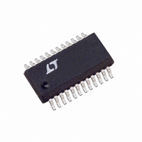
LTC3736EGN-1#PBF Linear Technology, LTC3736EGN-1#PBF Datasheet - Page 21

LTC3736EGN-1#PBF
Manufacturer Part Number
LTC3736EGN-1#PBF
Description
IC CTRLR SW SYNC DUAL 2PH 24SSOP
Manufacturer
Linear Technology
Series
PolyPhase®r
Type
Step-Down (Buck)r
Datasheet
1.LTC3736EGN-1.pdf
(28 pages)
Specifications of LTC3736EGN-1#PBF
Internal Switch(s)
No
Synchronous Rectifier
Yes
Number Of Outputs
2
Voltage - Output
0.6 ~ 9.8 V
Current - Output
1A
Frequency - Switching
450kHz ~ 580kHz
Voltage - Input
2.75 ~ 9.8 V
Operating Temperature
-40°C ~ 85°C
Mounting Type
Surface Mount
Package / Case
24-SSOP
Lead Free Status / RoHS Status
Lead free / RoHS Compliant
Power - Output
-
APPLICATIO S I FOR ATIO
modified slightly (from 0.2 to 5 times their suggested
values) to optimize transient response once the final PC
layout is done and the particular output capacitor type and
value have been determined. The output capacitors need
to be decided upon because the various types and values
determine the loop feedback factor gain and phase. An
output current pulse of 20% to 100% of full load current
having a rise time of 1µs to 10µs will produce output
voltage and I
overall loop stability. The gain of the loop will be increased
by increasing R
increased by decreasing C
behavior is related to the stability of the closed-loop
system and will demonstrate the actual overall supply
performance. For a detailed explanation of optimizing the
compensation components, including a review of control
loop theory, refer to Application Note 76.
A second, more severe transient is caused by switching in
loads with large (>1µF) supply bypass capacitors. The
discharged bypass capacitors are effectively put in parallel
with C
OUT
, causing a rapid drop in V
TH
pin waveforms that will give a sense of the
C
, and the bandwidth of the loop will be
U
U
C
. The output voltage settling
W
OUT
BOLD LINES INDICATE HIGH CURRENT PATHS
. No regulator can
Figure 11. LTC3736-1 Layout Diagram
10
11
12
1
2
3
4
5
6
7
8
9
SW1
IPRG1
V
I
IPRG2
FREQ
SGND
V
TRACK
V
I
PGOOD
TH1
TH2
FB1
IN
FB2
U
LTC3736EGN-1
SENSE1
SENSE2
RUN/SS
SSDIS
PGND
PGND
PGND
SW2
BG1
BG2
TG1
TG2
+
+
24
23
22
21
20
19
18
17
16
15
14
13
deliver enough current to prevent this problem if the load
switch resistance is low and it is driven quickly. The only
solution is to limit the rise time of the switch drive so that
the load rise time is limited to approximately (25)(C
Thus a 10µF capacitor would require a 250µs rise time,
limiting the charging current to about 200mA.
PC Board Layout Checklist
When laying out the printed circuit board, the following
checklist should be used to ensure proper operation of the
LTC3736-1. These items are illustrated in the layout dia-
gram of Figure 11. Figure 12 depicts the current wave-
forms present in the various branches of the 2-phase dual
regulator.
1) The power loop (input capacitor, MOSFETs, inductor,
output capacitor) of each channel should be as small as
possible and isolated as much as possible from the power
loop of the other channel. Ideally, the drains of the P- and
N-channel FETs should be connected close to one another
with an input capacitor placed across the FET sources
(from the P-channel source to the N-channel source) right
C
C
OUT1
OUT2
C
C
C
VIN1
VIN2
MN1
MN2
VIN
+
+
37361 F11
L1
L2
V
V
MP1
MP2
OUT1
OUT2
V
IN
LTC3736-1
21
LOAD
37361f
).


