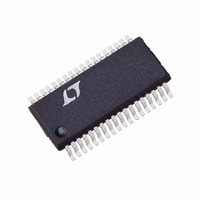
LTC3731HG Linear Technology, LTC3731HG Datasheet - Page 17

LTC3731HG
Manufacturer Part Number
LTC3731HG
Description
IC REG SW SYNC 3PH STPDWN 36SSOP
Manufacturer
Linear Technology
Series
PolyPhase®r
Type
Step-Down (Buck)r
Specifications of LTC3731HG
Internal Switch(s)
No
Synchronous Rectifier
Yes
Number Of Outputs
1
Voltage - Output
0.6 ~ 6 V
Frequency - Switching
225kHz ~ 680kHz
Voltage - Input
4 ~ 36 V
Operating Temperature
-40°C ~ 140°C
Mounting Type
Surface Mount
Package / Case
36-SSOP
Lead Free Status / RoHS Status
Contains lead / RoHS non-compliant
Current - Output
-
Power - Output
-
Lead Free Status / Rohs Status
Not Compliant
Available stocks
Company
Part Number
Manufacturer
Quantity
Price
Part Number:
LTC3731HG
Manufacturer:
LINEAR/凌特
Quantity:
20 000
Part Number:
LTC3731HG#PBF
Manufacturer:
LINEAR/凌特
Quantity:
20 000
Part Number:
LTC3731HG#TRPBF
Manufacturer:
LINEAR/凌特
Quantity:
20 000
applicaTions inForMaTion
available in case heights ranging from 2mm to 4mm. Other
capacitor types include Sanyo POS-CAP , Sanyo OS-CON,
Nichicon PL series and Sprague 595D series. Consult the
manufacturer for other specific recommendations.
R
Once the frequency and inductor have been chosen,
R
required peak inductor current. The current comparator
has a typical maximum threshold of 75mV/R
an input common mode range of SGND to (1.1) • V
The current comparator threshold sets the peak inductor
current, yielding a maximum average output current I
equal to the peak value less half the peak-to-peak ripple
current, ∆I
Allowing a margin for variations in the IC and external
component values yields:
The IC works well with values of R
0.02Ω.
V
The V
cuits of the controller and to the top and bottom gate
drivers. Therefore, they must be bypassed very carefully
to ground with ceramic capacitors, type X7R or X5R (de-
pending upon the operating temperature environment)
of at least 1µF immediately next to the IC and preferably
an additional 10µF placed very close to the IC due to the
extremely high instantaneous currents involved. The total
capacitance, taking into account the voltage coefficient
of ceramic capacitors, should be 100 times as large as
the total combined gate charge capacitance of ALL of the
MOSFETs being driven. Good bypassing close to the IC is
necessary to supply the high transient currents required
by the MOSFET gate drivers while keeping the 5V supply
quiet enough so as not to disturb the very small-signal
high bandwidth of the current comparators.
CC
SENSE
SENSE1
R
Decoupling
SENSE
CC
Selection for Output Current
, R
and V
L
SENSE2
=
.
N
DR
50
I
MAX
, R
mV
pins supply power to the internal cir-
SENSE3
are determined based on the
SENSE
from 0.002Ω to
SENSE
MAX
and
CC
.
Topside MOSFET Driver Supply (C
External bootstrap capacitors, C
BOOST pins, supply the gate drive voltages for the top-
side MOSFETs. Capacitor C
is charged though diode D
is low. When one of the topside MOSFETs turns on, the
driver places the C
desired MOSFET. This enhances the MOSFET and turns
on the topside switch. The switch node voltage, SW,
rises to V
MOSFET on, the boost voltage is above the input supply
(V
needs to be 30 to 100 times that of the total gate charge
capacitance of the topside MOSFET(s) as specified on the
manufacturer’s data sheet. The reverse breakdown of D
must be greater than V
The output voltage is set by an external resistive divider
according to the following formula:
The resistive divider is connected to the output as shown
in Figure 2.
Soft-Start/Run Function
The RUN/SS pin provides three functions: 1) ON/OFF , 2)
soft-start and 3) a defeatable short-circuit latch off timer.
Soft-start reduces the input power sources’ surge currents
by gradually increasing the controller’s current limit (pro-
portional to an internal buffered and clamped V
latchoff timer prevents very short, extreme load transients
from tripping the overcurrent latch. A small pull-up cur-
rent (>5µA) supplied to the RUN/SS pin will prevent the
overcurrent latch from operating. A maximum pull-up cur-
rent of 200µA is allowed into the RUN/SS pin even though
the voltage at the pin may exceed the absolute maximum
rating for the pin. This is a result of the limited current
and the internal protection circuit on the pin. The following
explanation describes how this function operates.
BOOST
V
OUT
= V
=
IN
0 6 1
CC
and the BOOST pin follows. With the topside
.
V
+ V
IN
B
+
). The value of the boost capacitor C
voltage across the gate-source of the
R
R
2
1
IN(MAX)
B
B
from V
in the Functional Diagram
.
B
B
CC
, connected to the
LTC3731H
, D
when the SW pin
B
)
ITH
). The
3731Hfb
B
B


